El display panel and el display apparatus comprising it

a technology of display panel and display device, which is applied in the direction of instruments, semiconductor devices, computing, etc., can solve the problems of display irregularities, difficulty in realizing a large-scale and high-definition display panel, and difficulty in controlling and a relatively high price, so as to suppress the variation in output current and improve quality.

Inactive Publication Date: 2005-03-17
PANASONIC CORP
View PDF17 Cites 344 Cited by
  • Summary
  • Abstract
  • Description
  • Claims
  • Application Information

AI Technical Summary

Benefits of technology

Bearing in mind the above-described problems, the present invention was made. Accordingly, an object of the present invention is to provide an EL display device capable of realizing image display of better quality by suppressing variation in output current from each output terminal of a source driver.
As a result of such arrangement, variation in output current from the source driver is suppressed, thereby realizing better image display.
Furthermore, in the above-described EL display device of the present invention, it is preferable that the source driver is provided with a light shielding film for preventing the first and second current sources from being illuminated with rays of light emitted from the EL elemental device. It becomes possible to avoid the photoconductor phenomenon caused by rays of light emitted from the EL elemental device falling upon the first and second current sources.
As a result of such arrangement, when a gray scale to be displayed is lower than a predetermined gray scale, display is carried out at increments of a lower current value, while, when a gray scale to be displayed is higher than a predetermined gray scale, display is carried out at increments of a higher current value. As the result of this, it becomes possible to provide the display characteristic that brightness variation is small in the low gray scale region whereas in the high gray scale region brightness variation is great, thereby making it possible to display an image natural to human eyes.
In addition, in the above-described EL display device of the present invention, it is preferable that the source driver is provided with a light shielding film for preventing the first and second current output circuits from being illuminated with rays of light emitted from the EL elemental device.

Problems solved by technology

Though the former configuration is simple in structure, it has a difficulty in realizing a large-scale and high-definition display panel.
However, it has problems of a technical difficulty in control and of a relatively high price.
Since organic EL devices emit light based on current, the organic EL display panel involves a problem that display irregularities occur if there are variations in transistor characteristics.
Further, a conventional EL display panel cannot sufficiently charge / discharge the parasitic capacitance which is present in the source signal line 18.
For this reason there arises a problem that in some cases a desired current cannot be fed to pixel 16.
This creates variations in output current from each output terminal, thereby producing the problem that image display of better quality is not obtained.
If, in a source driver of the current driven type, display is carried out at a constant current value increment, this represents the problem that it is impossible to provide image display natural to human eyes.

Method used


Image

  • El display panel and el display apparatus comprising it
  • El display panel and el display apparatus comprising it
  • El display panel and el display apparatus comprising it

Examples


Embodiment Construction

Hereinafter, embodiments of the present invention will be described with reference to the drawings.

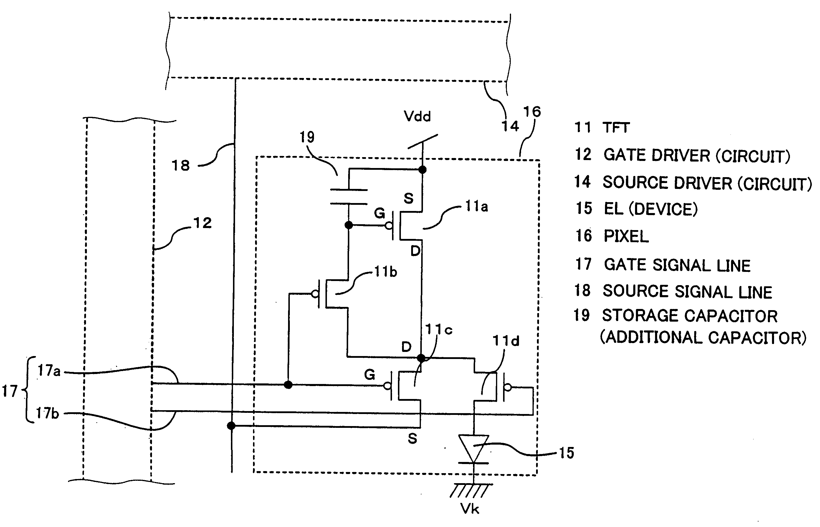
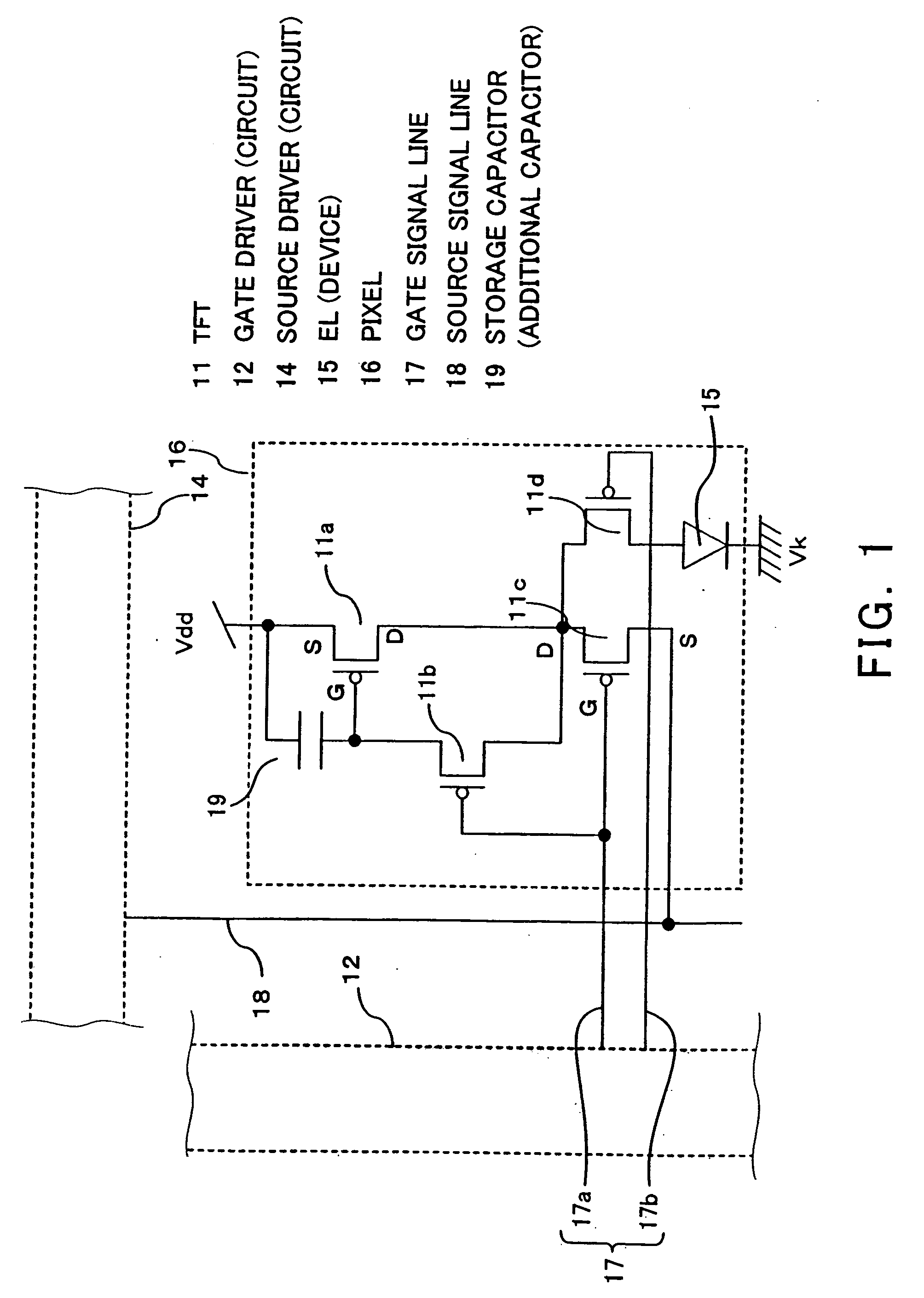
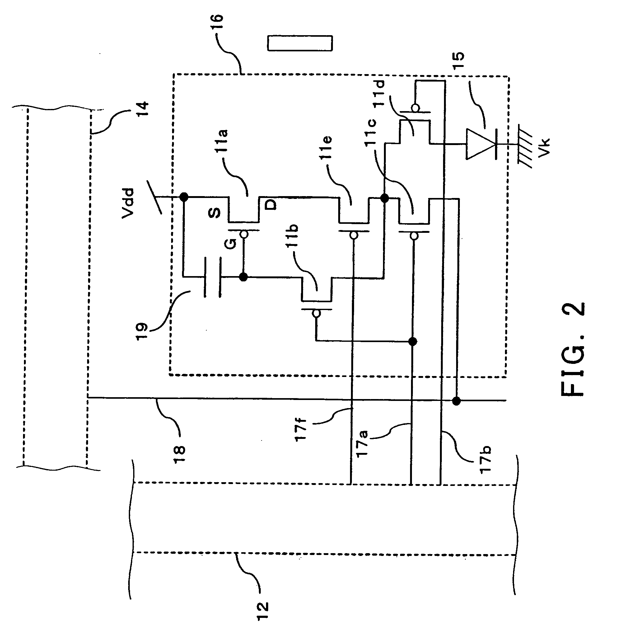
For easy understanding and / or illustration, each of the drawings in this description may have portions omitted and / or enlarged / reduced. For example, an encapsulating film 111 and the like are shown to be quite thick in the sectional view of a display panel at FIG. 11. On the other hand, an encapsulating cover 85 is shown to be thin in FIG. 10. There are omitted portions. For example, a display panel or the like according to the present invention needs to have a phase film such as a circularly polarizing plate for antireflection. However, such a phase film is omitted from the drawings used in this description. This holds true for other drawings. Like numerals, characters or the like designate parts having identical or similar forms, materials, functions or operations.

It is to be noted that the details to be described with reference to the drawings may be combined with other embodim...


PUM


Abstract

In a source driver (14) provided in an electroluminescent (EL) display device of the present invention, the gate voltage of a first-stage current source formed by a transistor (631) is applied to the gate of a transistor (632a) which is a second-stage current source situated next to the transistor (631) and, as a result, a current flowing through the transistor (632a) is transferred to a transistor (632b) which is a second-stage current source. In addition, the gate voltage of the transistor (632b) is applied to the gate of a transistor (633a) which is a third-stage current source situated next to the transistor (632b) and, as a result, a current flowing through the transistor (633a) is transferred to a transistor (633b) which is a third-stage current source. The gate of the transistor (633b) is provided with a large number of current sources (634) corresponding to the number of bits required.

Description

TECHNICAL FIELD The present invention relates to an EL display apparatus employing an organic or inorganic electroluminescence (EL) device and, more particularly, to an EL display apparatus capable of feeding an EL device with a desired current, a method of driving the same, and an electronic apparatus provided with such an EL display apparatus. BACKGROUND ART In general, an active-matrix display apparatus has a multiplicity of pixels arranged in matrix and displays an image by controlling the intensity of light pixel by pixel in accordance with image signals given. When, for example, liquid crystal is used as an electro-optic substance, the transmittance of each pixel varies in accordance with the voltage applied to the pixel. The basic operation of an active-matrix image display apparatus employing an organic electroluminescence (EL) material as an electro-optic converting substance is the same as in the case where liquid crystal is used. A liquid crystal display panel has pixe...

Claims


Application Information

Patent Timeline
Patent Type & Authority Applications(United States)
IPC IPC(8): G09G3/32H01L27/32
CPCG09G3/3241H01L27/3244G09G3/3266G09G3/3283G09G2300/0426G09G2300/0809G09G2300/0814G09G2300/0819G09G2300/0842G09G2300/0852G09G2300/0861G09G2310/0205G09G2310/0218G09G2310/0248G09G2310/0251G09G2310/0256G09G2310/0267G09G2310/027G09G2320/0261G09G2320/0276G09G2320/041G09G2320/043H01L27/3213G09G3/325H10K59/351H10K59/12G09G3/30
Inventor YAMANO, ATSUHIROTAKAHARA, HIROSHITSUGE, HITOSHI
Owner PANASONIC CORP
Why Eureka
Try Eureka