

Vertical GaN light emitting diode and method for manufacturing the same
a technology of light-emitting diodes and vertical gans, which is applied in the direction of basic electric elements, electrical equipment, semiconductor devices, etc., can solve the problems of limiting the structure of gan light-emitting diodes, and no practical technique for forming bulk single crystals of gan, so as to improve the current density distribution
- Summary
- Abstract
- Description
- Claims
- Application Information
AI Technical Summary
Benefits of technology
Problems solved by technology
Method used
Image

Examples
Embodiment Construction
[0032] Now, preferred embodiments of the present invention will be described in detail with reference to the annexed drawings.
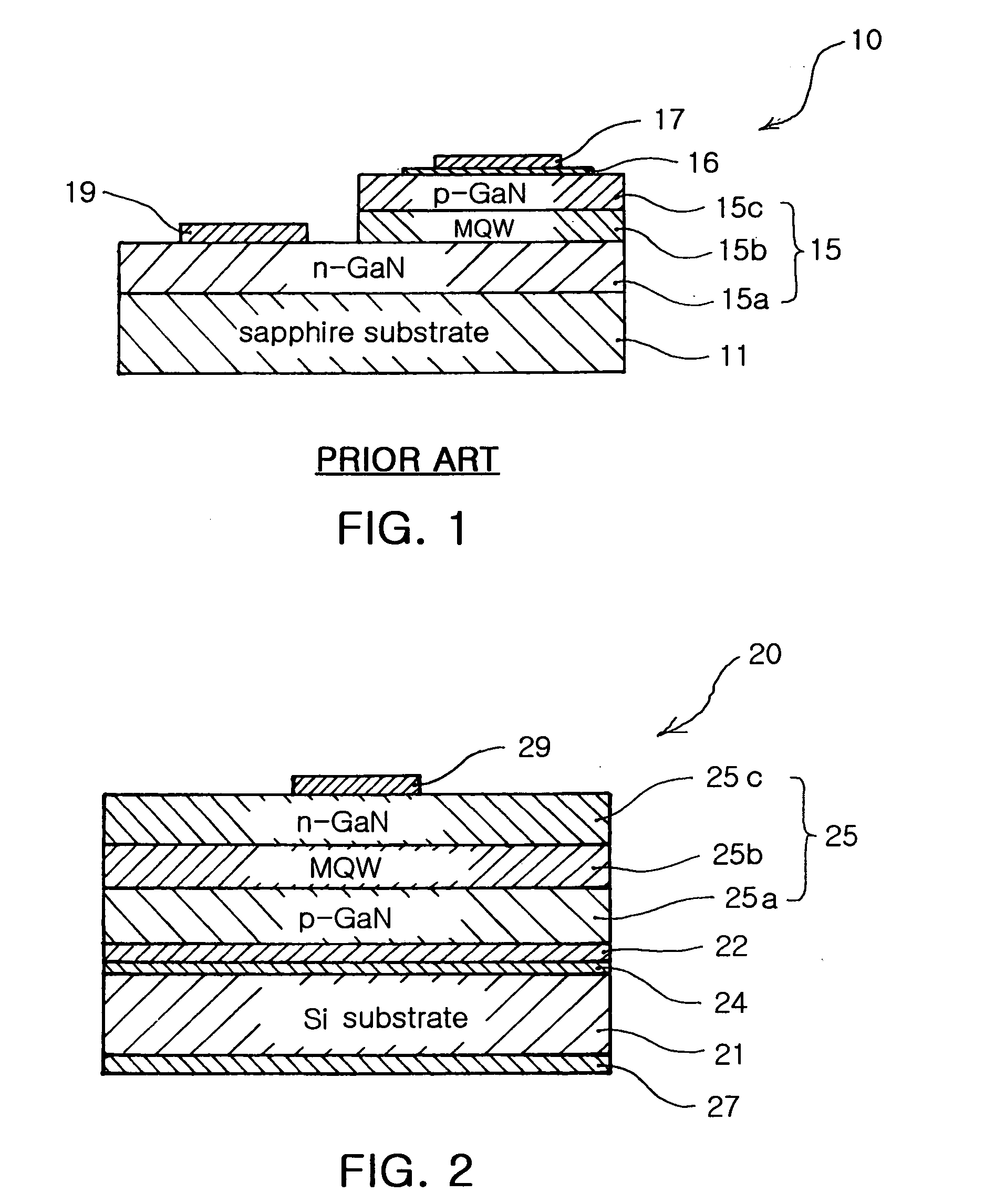
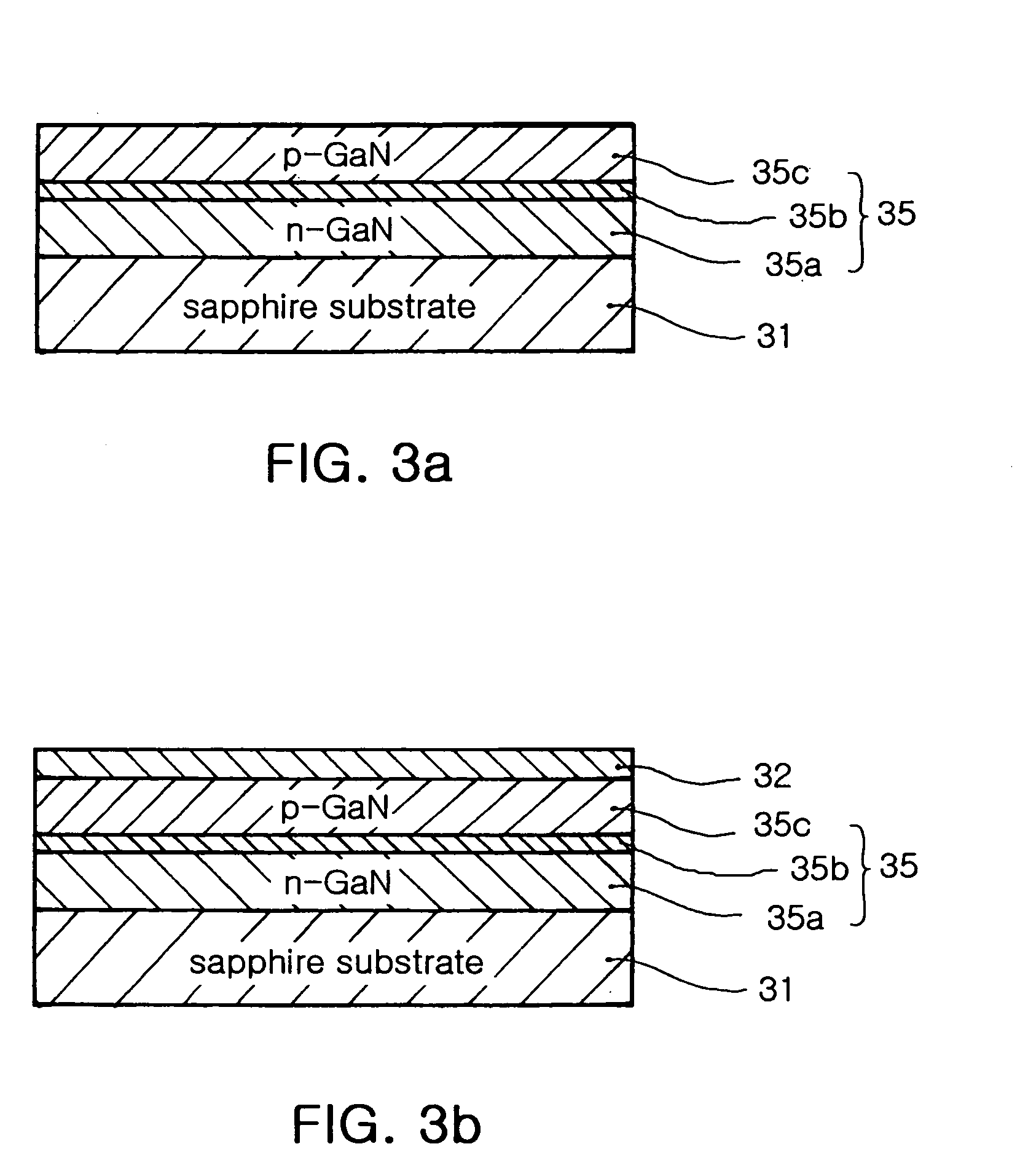
[0033]FIG. 2 is a cross-sectional view of a vertical GaN light emitting diode 20 in accordance with one preferred embodiment of the present invention.
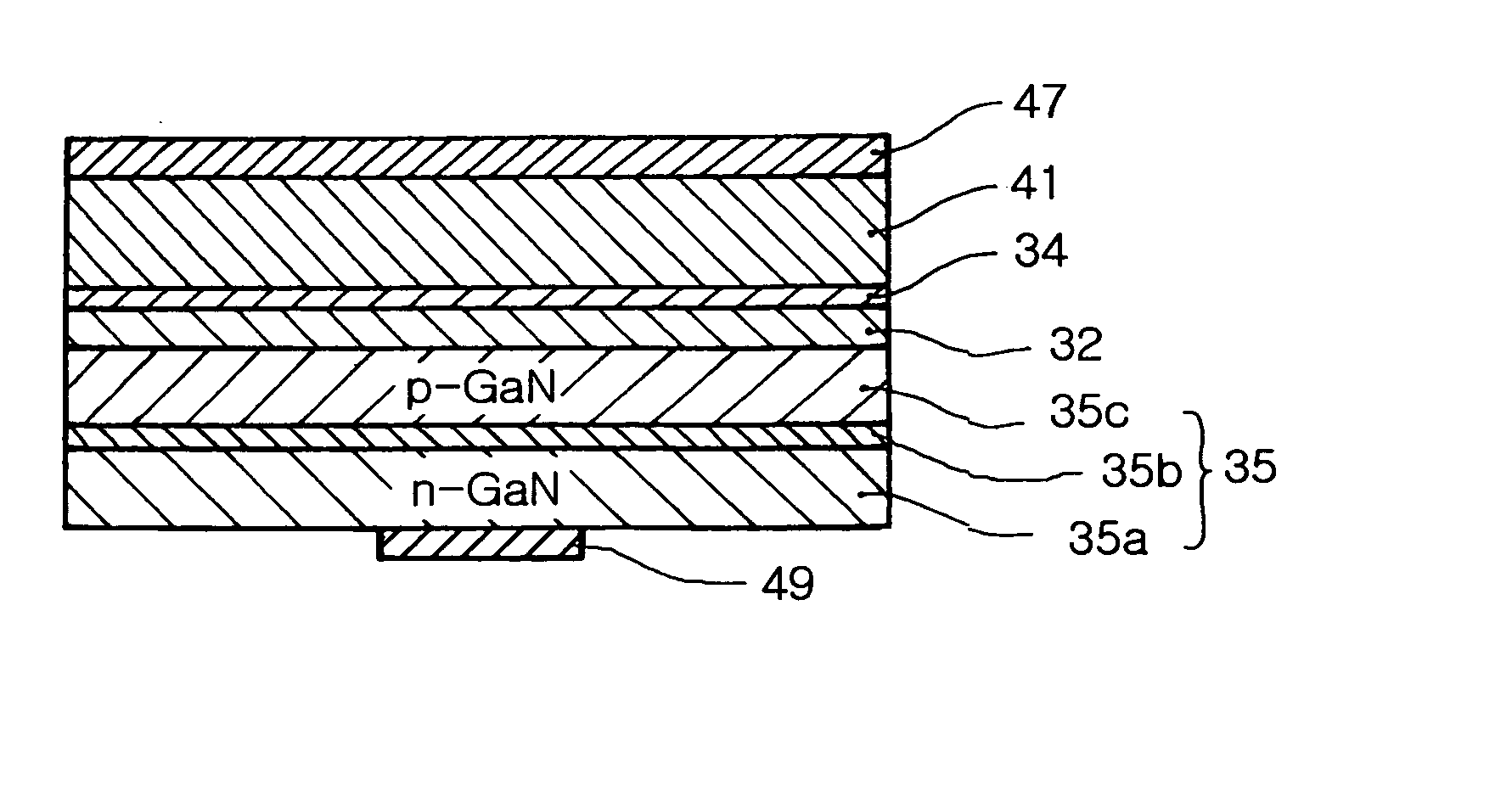
[0034] The vertical GaN light emitting diode 40 comprises a light emitting structure 25 including a p-type GaN clad layer 25a, an active layer 25b, and an n-type GaN clad layer 25c. Further, the GaN light emitting diode 40 selectively comprises a reflective layer 22 formed on the lower surface of the p-type GaN clad layer 25a. The reflective layer 22 is attached to a silicon substrate 21 using a conductive adhesive layer 24. The reflective layer 22 serves to improve the effective luminance depending on light emitted from the upper surface of the GaN light emitting diode 20, and is made of a metal with high reflectivity. Preferably, the reflective layer 22 is made of a material selected from the group consistin...
PUM
 Abstract
Description
Claims
Application Information