Liquid crystal display device and manufacturing method thereof

a technology of liquid crystal display and manufacturing method, which is applied in non-linear optics, instruments, optics, etc., can solve the problems of reducing display quality and reducing the yield rate of manufacture, and achieves the effect of high display quality and invisible luminance point defects

Active Publication Date: 2010-08-12
SHARP KK
View PDF3 Cites 1 Cited by
  • Summary
  • Abstract
  • Description
  • Claims
  • Application Information

AI Technical Summary

Benefits of technology

[0027]In accordance with the present invention, the liquid crystal display device having the higher display quality with the luminance point defect certainly invisible.

Problems solved by technology

The luminance point defect extremely reduces the display quality and decreases the yield rate of manufacture.

Method used


Image

  • Liquid crystal display device and manufacturing method thereof
  • Liquid crystal display device and manufacturing method thereof
  • Liquid crystal display device and manufacturing method thereof

Examples


Embodiment Construction

[0035]An embodiment in accordance with the present invention will be described with reference to FIGS. 1 through 6.

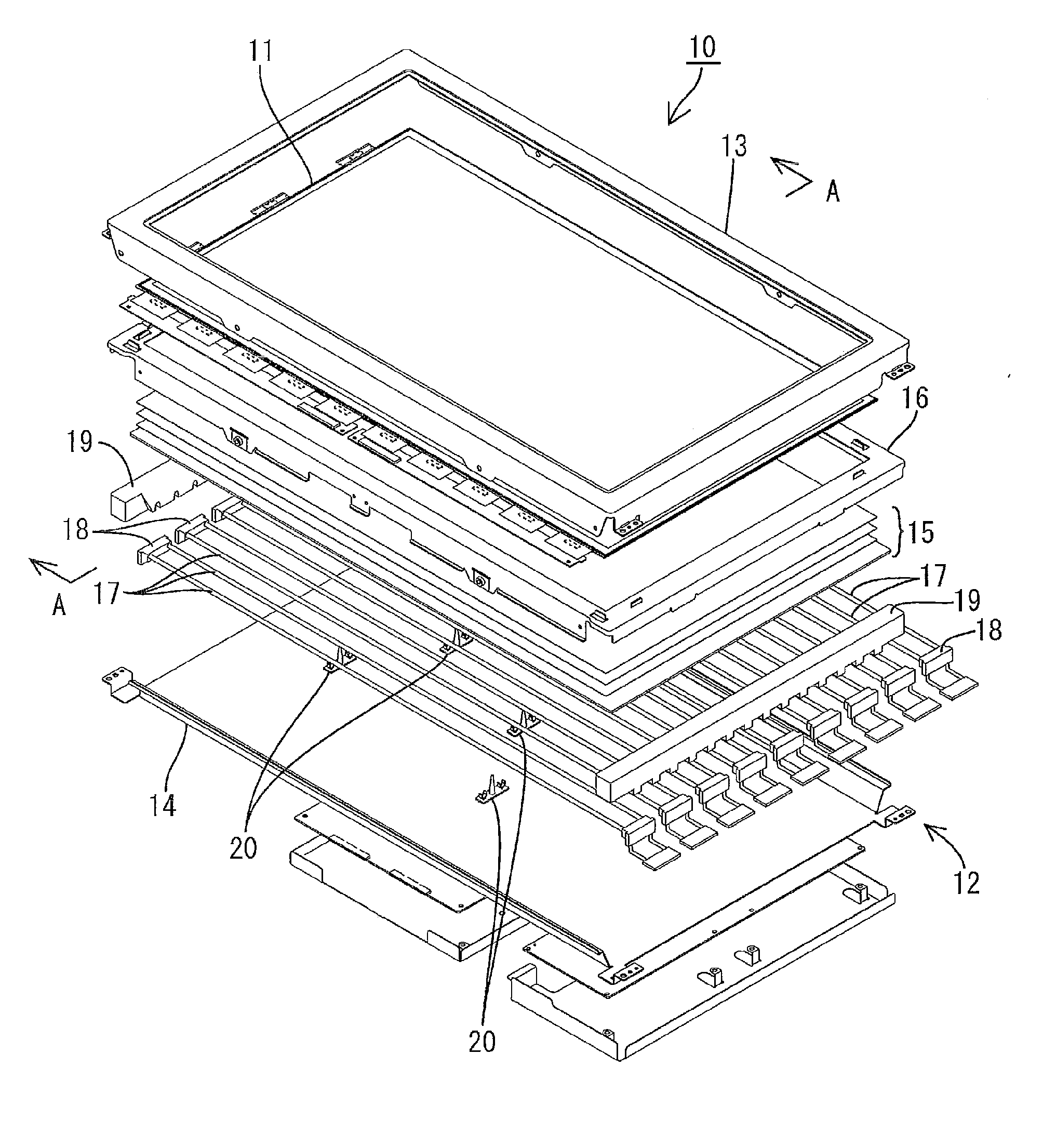
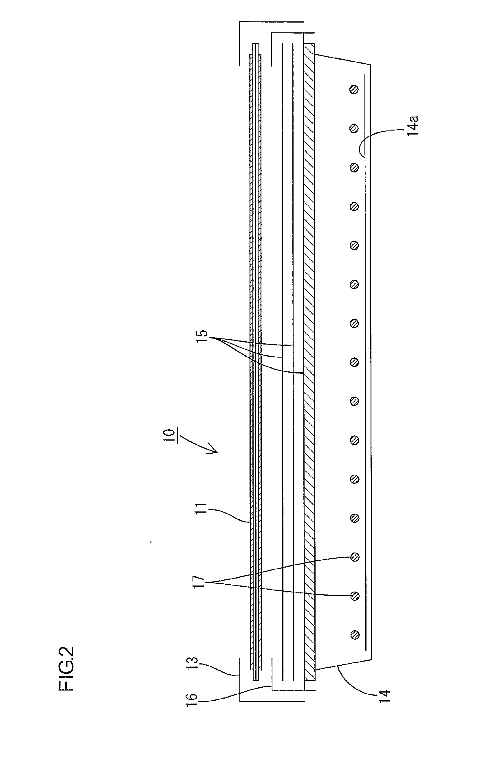
[0036]FIG. 1 is a perspective view illustrating a schematic configuration of a liquid crystal display device of this embodiment; FIG. 2 is a sectional view of the liquid crystal display device of FIG. 1 taken on line A-A; FIG. 3 is a sectional view of a main part of a liquid crystal panel that the liquid crystal display device of FIG. 1 includes; FIG. 4 is an explanatory view illustrating an operational effect that the liquid crystal display device of this embodiment produces; FIG. 5 is an explanatory view illustrating a state of a lighting inspection step for an inspection-object liquid crystal panel; and FIG. 6 is a side view illustrating a schematic configuration of a luminance point defect compensating device.

[0037]First, a general configuration of a liquid crystal display device 10 of this embodiment will be described. As illustrated in FIGS. 1 and 2, the liquid cr...


PUM

PropertyMeasurementUnit
sizeaaaaaaaaaa
diameteraaaaaaaaaa
wavelength rangeaaaaaaaaaa

Abstract

A liquid crystal display device 10 in accordance with the present invention includes a liquid crystal 11 and a lighting device 12, the liquid crystal panel 11 having a liquid crystal layer 50 provided between a pair of glass substrates 31, 41, the lighting device 12 supplying illumination light to the liquid crystal panel 11. The liquid crystal display device 10 is characterized in that a metal-halide containing region 60 is formed in a position in one of the pair of glass substrates 31, 41. The metal-halide containing region 60 contains a crystal of metal halide which exhibits photochromism in the light supplied from the lighting device 12. The position is capable of blocking light toward a luminance point defect occurrence portion X that becomes a cause of a luminance point defect. The one of the pair of glass substrates 31, 41 is disposed on the lighting device 12 side.

Description

TECHNICAL FIELD[0001]The present invention relates to a liquid crystal display device and a manufacturing method thereof.BACKGROUND ART[0002]There is a method of manufacturing a liquid crystal device, which is such as follows: providing a switching element (for example, TFTs), pixel electrodes, etc. on one of a pair of glass substrates; providing a counter electrode etc. on the other one of the glass substrates and, thereafter, laminating the two glass substrates via a spacer; next, injecting liquid crystal into a space between the two glass substrates to form a liquid crystal layer and, thereafter, laminating polarizing plates onto surfaces of the two glass substrates to obtain a liquid crystal panel; finally, mounting a lighting device including, for example, a plurality of cold cathode tubes as a light source to the liquid crystal panel.[0003]The above-explained process of manufacturing the liquid crystal device can include a step of detecting inferiority by operating various kin...

Claims


Application Information

Patent Timeline
Patent Type & Authority Applications(United States)
IPC IPC(8): G02F1/1335G02F1/13
CPCG02F1/1309G02F2202/14G02F2201/508G02F1/133604
Inventor IKEDA, MASAKI
Owner SHARP KK
Why Eureka
Try Eureka