

Touch screen panel and method for manufacturing the same, and display device
- Summary
- Abstract
- Description
- Claims
- Application Information
AI Technical Summary
Benefits of technology
Problems solved by technology
Method used
Image

Examples
Embodiment Construction
[0026]The specific embodiments of a touch screen panel and a method for manufacturing the same, and a display device according to the embodiments of the invention will be illustrated in detail below in conjunction with the drawings.
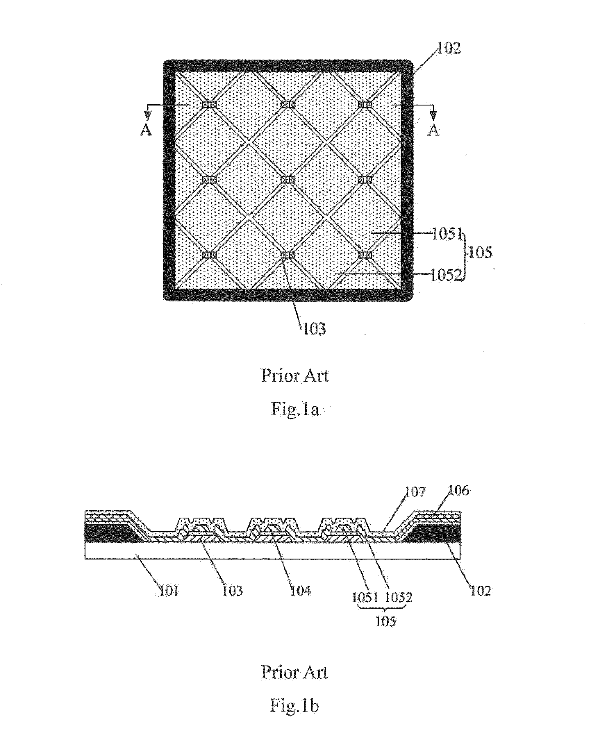
[0027]In the drawings, the thickness of each layer of thin film and the size and shape of each region do not reflect the real proportion; instead, they are only used for schematically illustrating the contents of the invention.
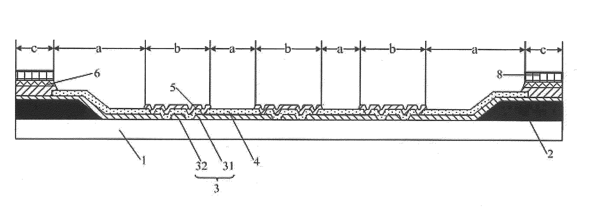
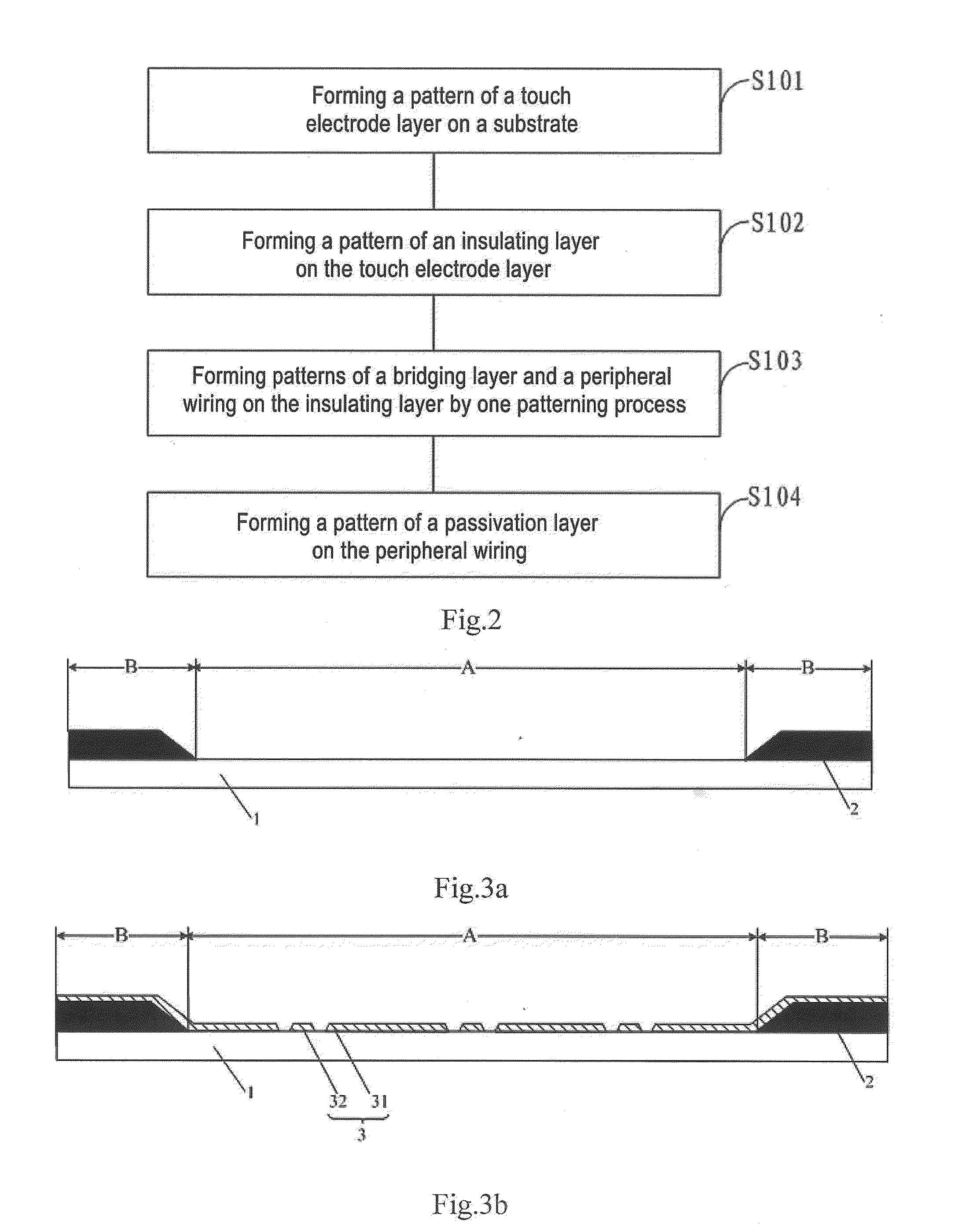
[0028]According to one embodiment of the invention, there provides a method for manufacturing a touch screen panel, as shown in FIG. 2, which specifically includes the steps of:[0029]Step S101: forming a pattern of a touch electrode layer 3 on a substrate 1, wherein the touch electrode layer 3 includes a touch sensing electrode 31 and a touch driving electrode 32 that are formed crosswise and insulated from each other, and as shown in FIG. 3b, the touch electrode layer 3 has a pattern in both a touch region A and a non-touch region ...
PUM
| Property | Measurement | Unit |
|---|---|---|
| Electrical conductor | aaaaa | aaaaa |
| Transparency | aaaaa | aaaaa |
| Photosensitivity | aaaaa | aaaaa |
Abstract
Description
Claims
Application Information