Pixel and display device having the same

a display device and pixel technology, applied in semiconductor devices, electrical devices, instruments, etc., can solve the problems of insufficient luminance of the pixel, change in the gate voltage of the driving transistor, and leakage current that may occur in the switching transistor of the pixel, so as to achieve effective reduction or prevention of leakage current, improve image quality of the display device, and improve the effect of grayscale expression of the pixel

Pending Publication Date: 2021-02-25
SAMSUNG DISPLAY CO LTD
View PDF1 Cites 4 Cited by
  • Summary
  • Abstract
  • Description
  • Claims
  • Application Information

AI Technical Summary

Benefits of technology

[0027]According to the pixel and the display device having the same according to embodiments, a leakage current that may occur in the switching transistor of the pixel may be effectively reduced or prevented. Therefore, grayscale expression of the pixel may be increased, and image quality of the display device may be improved.

Problems solved by technology

However, a leakage current may occur in the pixel due to a characteristic of the transistors.
The leakage current may cause a change in a gate voltage of the driving transistor.
Therefore, the desired luminance may not be sufficiently expressed in the pixel.

Method used


Image

  • Pixel and display device having the same
  • Pixel and display device having the same
  • Pixel and display device having the same

Examples


Embodiment Construction

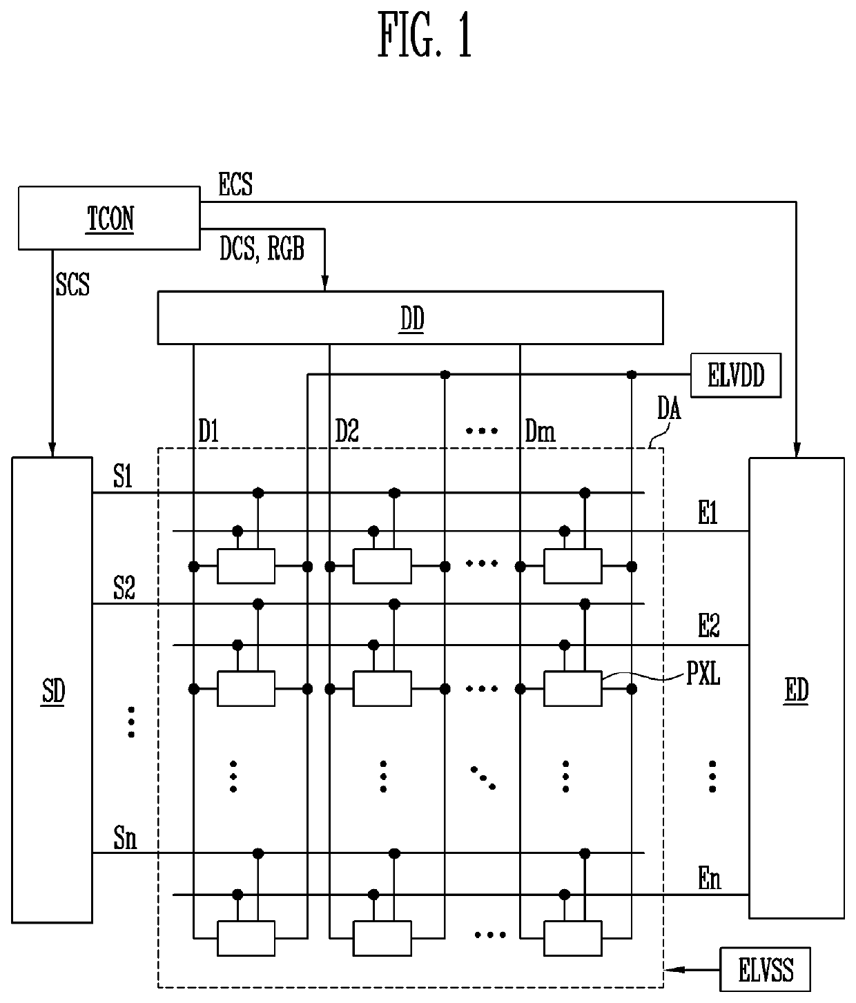
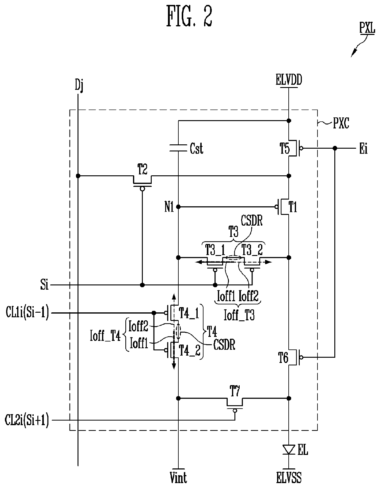
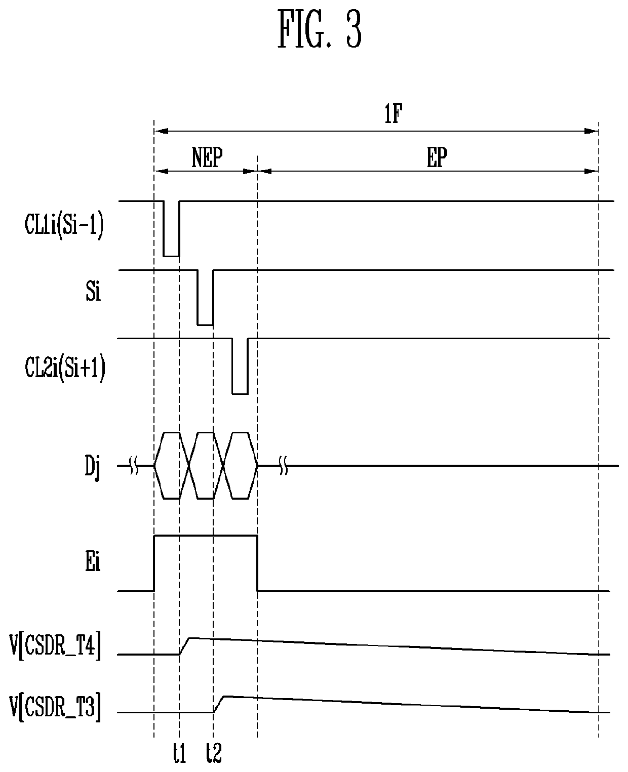
[0039]The disclosure may be modified in various ways and may have various forms, and embodiments will be illustrated in the drawings and described in detail herein. In the following description, the singular forms also include the plural forms unless the context clearly includes the singular.

[0040]The disclosure is not limited to the embodiments disclosed below, and may be modified in various forms and may be implemented in various modes. Each of the embodiments disclosed below may be implemented alone or in combination with at least one of any or all of the other embodiments.

[0041]In the drawings, some components which are not directly related to a characteristic of the disclosure may be omitted to clearly represent the disclosure. In addition, some components in the drawings may be shown to be exaggerated in size or proportion for clarity and for ease of description thereof. Throughout the drawings, the same or similar components will be given by the same reference numerals and sy...


PUM

PropertyMeasurementUnit
frequencyaaaaaaaaaa
voltageaaaaaaaaaa
conductiveaaaaaaaaaa

Abstract

A display device includes pixels at least one of which includes a light emitting element connected between a first power source and a second power source, a first transistor connected between the first power source and the light emitting element and controlling a driving current flowing through the light emitting element in response to a voltage of a first node, a switching transistor connected to the first node and including and active layer that includes first and second conductive regions spaced apart from each other, first and second channel regions disposed between the first and second conductive regions, and a common conductive region disposed between the first and second channel regions, and a conductive pattern overlapping the active layer to face the common conductive region.

Description

CROSS-REFERENCE TO RELATED APPLICATIONS[0001]This application claims priority to and benefits of Korean Patent Application No. 10-2019-0101682 under 35 U.S.C. § 119, filed in the Korean Intellectual Property Office on Aug. 20, 2019, the entire contents of which are incorporated herein by reference.BACKGROUND1. Technical Field[0002]Embodiments relate to a pixel and a display device having the same.2. Description of the Related Art[0003]A display device displays an image using pixels disposed in a display area. The pixels may be connected to respective scan lines and data lines, and may include transistors. For example, a pixel of an active light emitting display device may include a light emitting element, a driving transistor, and at least one switching transistor.[0004]In order to express a desired luminance in the pixels during a light emission period of each frame, a gate voltage of the driving transistor is required to be stably maintained. However, a leakage current may occur i...

Claims


Application Information

Patent Timeline
Patent Type & Authority Applications(United States)
IPC IPC(8): H01L27/32G09G3/3233G09G3/3291G09G3/3266
CPCH01L27/3276G09G3/3233G09G2320/0233G09G3/3266G09G3/3291G09G3/3208G09G2320/0271G09G2300/0842G09G2300/0861G09G2300/0819G09G2320/045G09G2320/0214H01L27/124H01L27/1251H10K59/1213G09G2300/0439G09G2320/02H10K59/12H10K59/131
Inventor KIM, KEUN WOOKIM, SANG SUBKWAK, HYE NAKIM, DOO NANGUYEN, THANH TIENLEE, YONG SUCHU, JAE HWAN
Owner SAMSUNG DISPLAY CO LTD
Why Eureka
Try Eureka