Display device and method of reparing the same

Pending Publication Date: 2022-10-27
SAMSUNG DISPLAY CO LTD
View PDF0 Cites 0 Cited by
  • Summary
  • Abstract
  • Description
  • Claims
  • Application Information

AI Technical Summary

Benefits of technology

The patent is about a defect that can occur in a pixel circuit of a display device. When this defect happens, the light-emitting element in that pixel always generates light, even when there is no scan or data signal. This results in a bright spot defect, which can impact the quality of the display. With the rise in display device size and resolution, this defect has become more common. The technical effect of the patent is to provide a solution to prevent these bright spot defects and ensure better quality of the display.

Problems solved by technology

Meanwhile, in a process of manufacturing the display device, a defect may occur in some pixel circuits.
A defect, for example, a short-circuit or opening of a thin-film transistor or a signal line of a pixel circuit may occur.
A pixel always emitting light as described above may be recognized as a bright spot to a user, causing a bright spot defect of the display device.
In particular, with the recent increase in size and high resolution of display devices, the possibility of such a defect in the pixel circuit and a bright spot defect of the display device has increased.

Method used


Image

  • Display device and method of reparing the same
  • Display device and method of reparing the same
  • Display device and method of reparing the same

Examples


Embodiment Construction

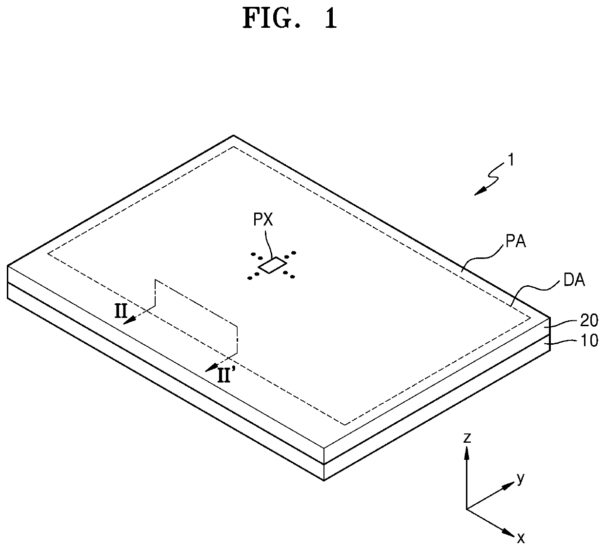
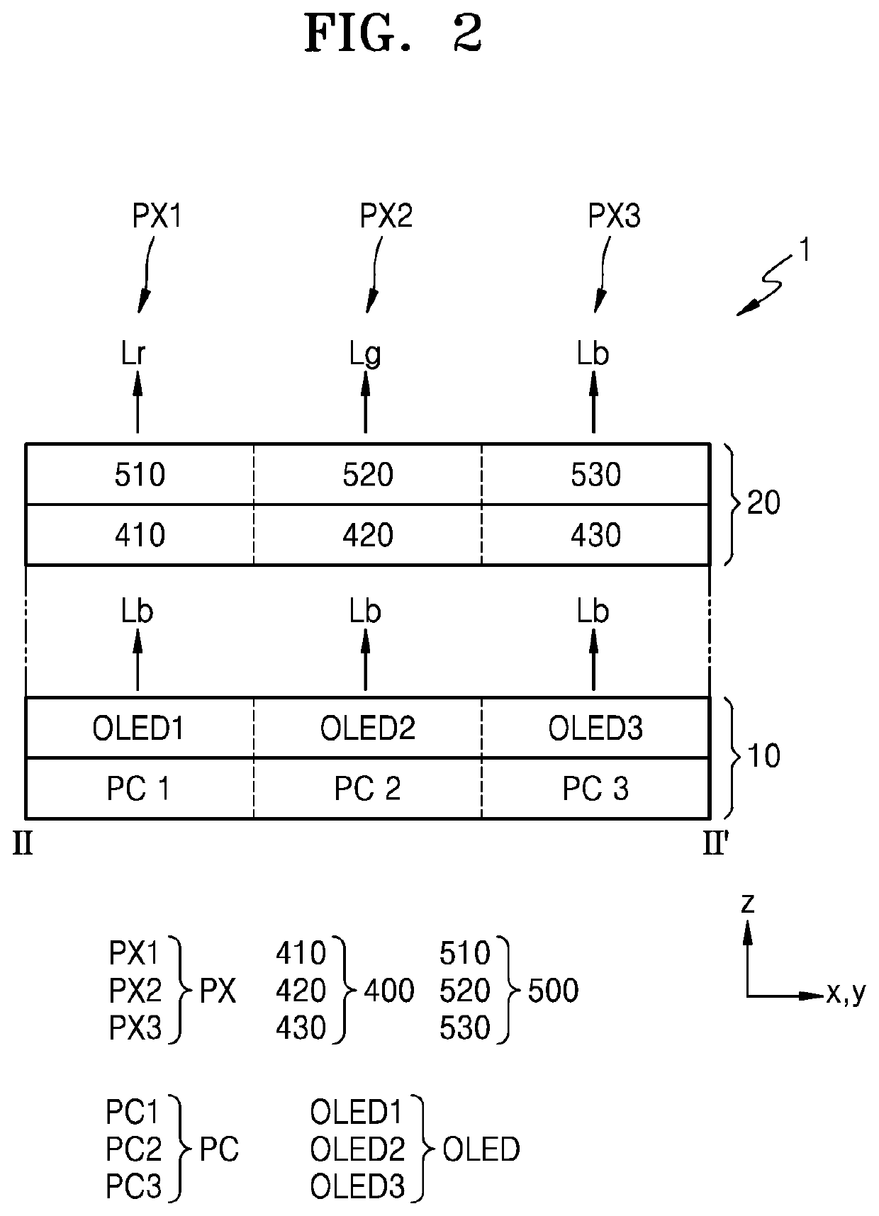
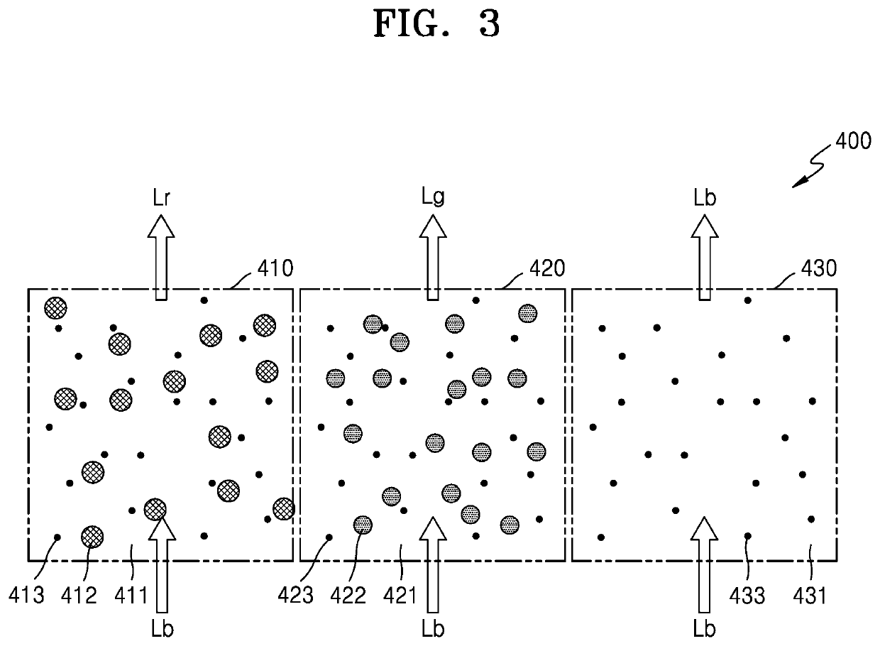
[0045]Reference will now be made in detail to embodiments, examples of which are illustrated in the accompanying drawings, wherein like reference numerals refer to like elements throughout the present disclosure. In this regard, the present embodiments may have different forms and configuration and should not be construed as being limited to the descriptions set forth herein. Accordingly, the embodiments are merely described below, by referring to the figures, to explain aspects of the present disclosure. As used herein, the term “and / or” includes any and all combinations of one or more of the associated listed items. Throughout the present disclosure, the expression “at least one of a, b or c” indicates only a, only b, only c, both a and b, both a and c, both b and c, all of a, b, and c, or any variations thereof.

[0046]Because the present disclosure may have diverse modified embodiments, embodiments are illustrated in the drawings and are described with respect to the embodiments. ...


PUM


Abstract

Provided are a display device in which a bright spot occurring due to a defective pixel circuit may be repaired into a dark spot, and a method of repairing the display device. The display device includes a substrate, a thin-film transistor arranged on the substrate and including a semiconductor layer and a gate electrode overlapping at least a portion of the semiconductor layer, a pixel electrode on the substrate, a node connection line connecting the thin-film transistor and the pixel electrode to each other, and an initialization voltage line arranged on the substrate and extending in a first direction, wherein the node connection line includes a repair portion overlapping the initialization voltage line in a plan view.

Description

CROSS-REFERENCE TO RELATED APPLICATION[0001]This application is based on and claims priority under 35 U.S.C. § 119 to Korean Patent Application No. 10-2021-0054632, filed on Apr. 27, 2021, in the Korean Intellectual Property Office, the disclosure of which is incorporated by reference herein in its entirety.BACKGROUND1. Field[0002]The present disclosure generally relates to a display device. More particularly, the present disclosure relates to a display device having a structure capable of a darkening repair when a bright spot defect occurs, and a method of repairing the display device.2. Description of the Related Art[0003]Display devices provide visual information such as images or videos to a user. With the development of various electronic devices such as televisions, computers, mobile phones, and tablet personal computers (PCs), display devices of various types applicable thereto have been developed.[0004]Such a display device includes a scan line and a data line insulated from...

Claims


Application Information

Patent Timeline
IPC IPC(8): H01L51/56H01L27/32
CPCH01L51/56H01L27/322H01L27/3265H01L27/3272H01L27/3276H01L2251/568H10K59/123H10K59/131H10K59/38H10K59/1216H10K59/126H10K71/861H01L27/124G09G2300/0426H10K59/88H10K71/00
Inventor JEON, YOUNGJAELEE, WOOGEUN
Owner SAMSUNG DISPLAY CO LTD
Why Eureka
Try Eureka