

Organic bistable element, organic bistable memory device using the same, and method for driving said organic bistable element and organic bistable memory device
Inactive Publication Date: 2008-04-08
DAI NIPPON PRINTING CO LTD
View PDF2 Cites 14 Cited by
- Summary
- Abstract
- Description
- Claims
- Application Information
AI Technical Summary
Benefits of technology
[0016]According to the present invention, an organic bistable element with a simple structure and having a low switching voltage can be realized by adopting a structure comprising an organic thin film interposed between a pair of electrodes and using a predetermined imidazole compound as a material for the organic thin film.
[0017]Further, accordin
Problems solved by technology
The organic bistable element disclosed in Japanese Patent Laid-Open No. 345431/2001 suffers from a problem that, due to a relatively high switching voltage, power consumption in driving is increased.
However, due to the three-layer structure of the laminate sandwitched between the pair of electrodes, the organic bistable element disadvan
Method used
View moreImage
Smart ImageViewing Examples

Examples
 PUM
 Abstract
There are provided an organic bistable element, which is simple in structure, can eliminate the need to increase production process steps, and has a low switching voltage, a memory device using the same, and a method for driving the organic bistable element and the memory device. The organic bistable element has a laminate structure comprising an organic thin film interposed between a first electrode and a second electrode. The organic thin film comprises an organic compound represented by formula (I):
Description
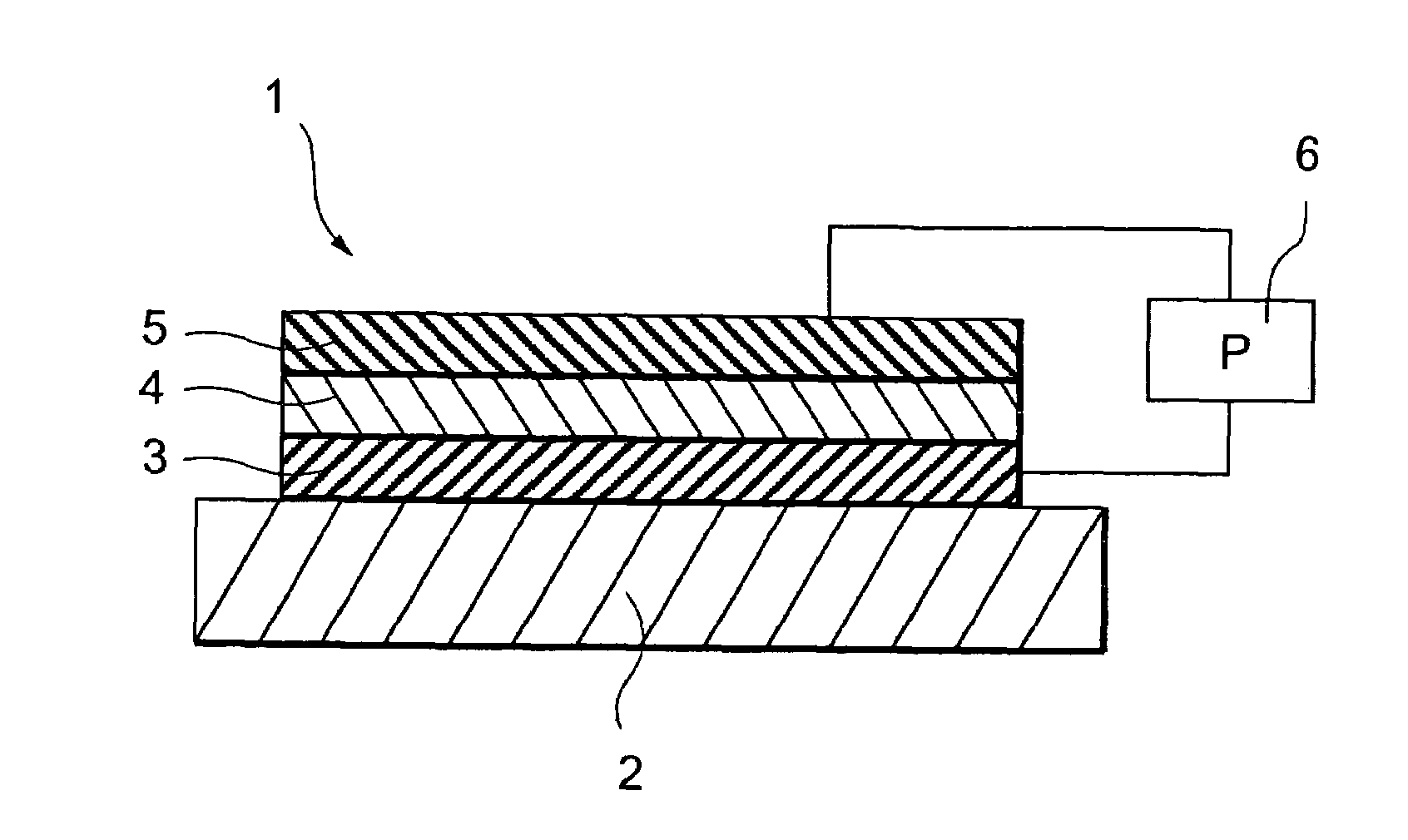
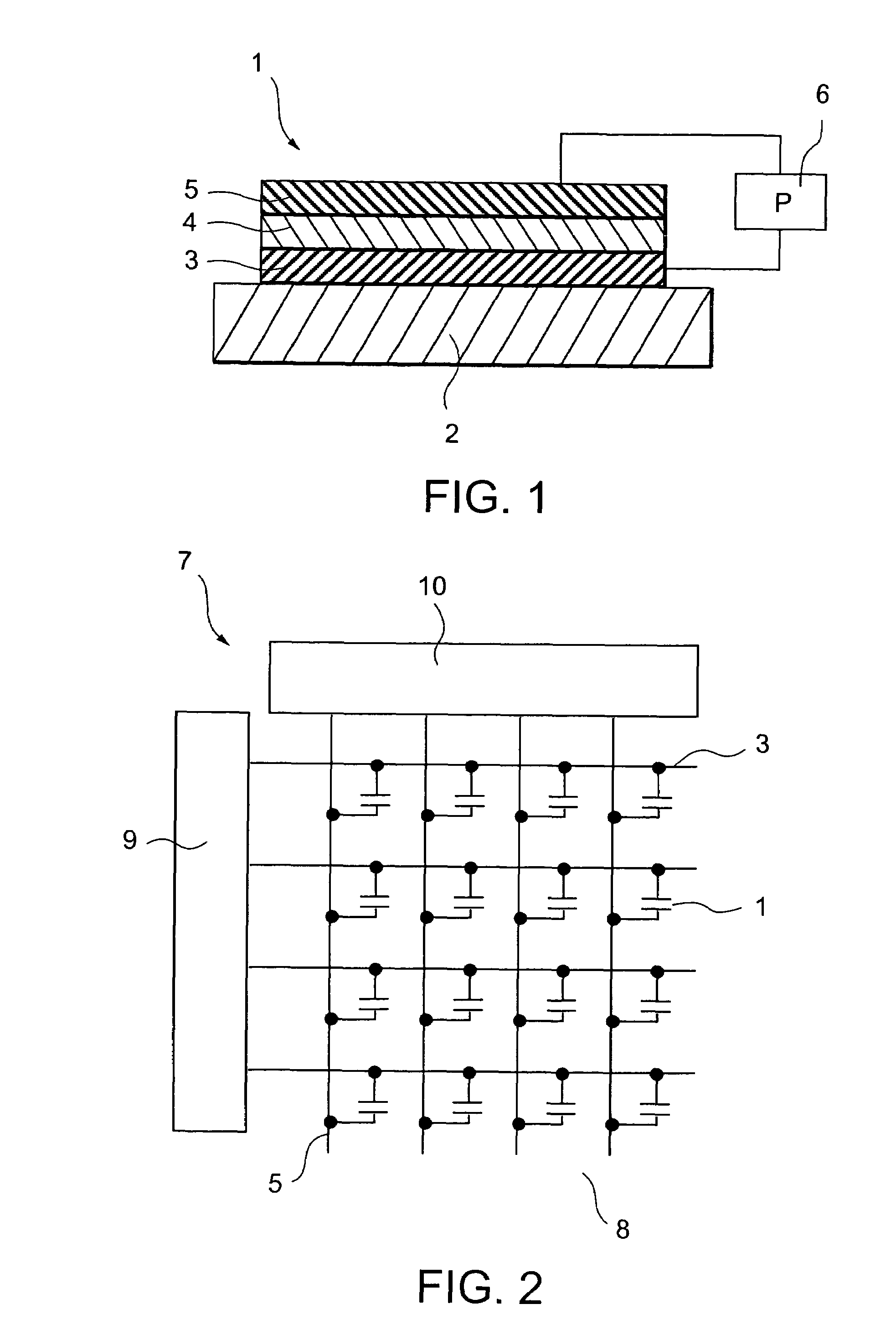
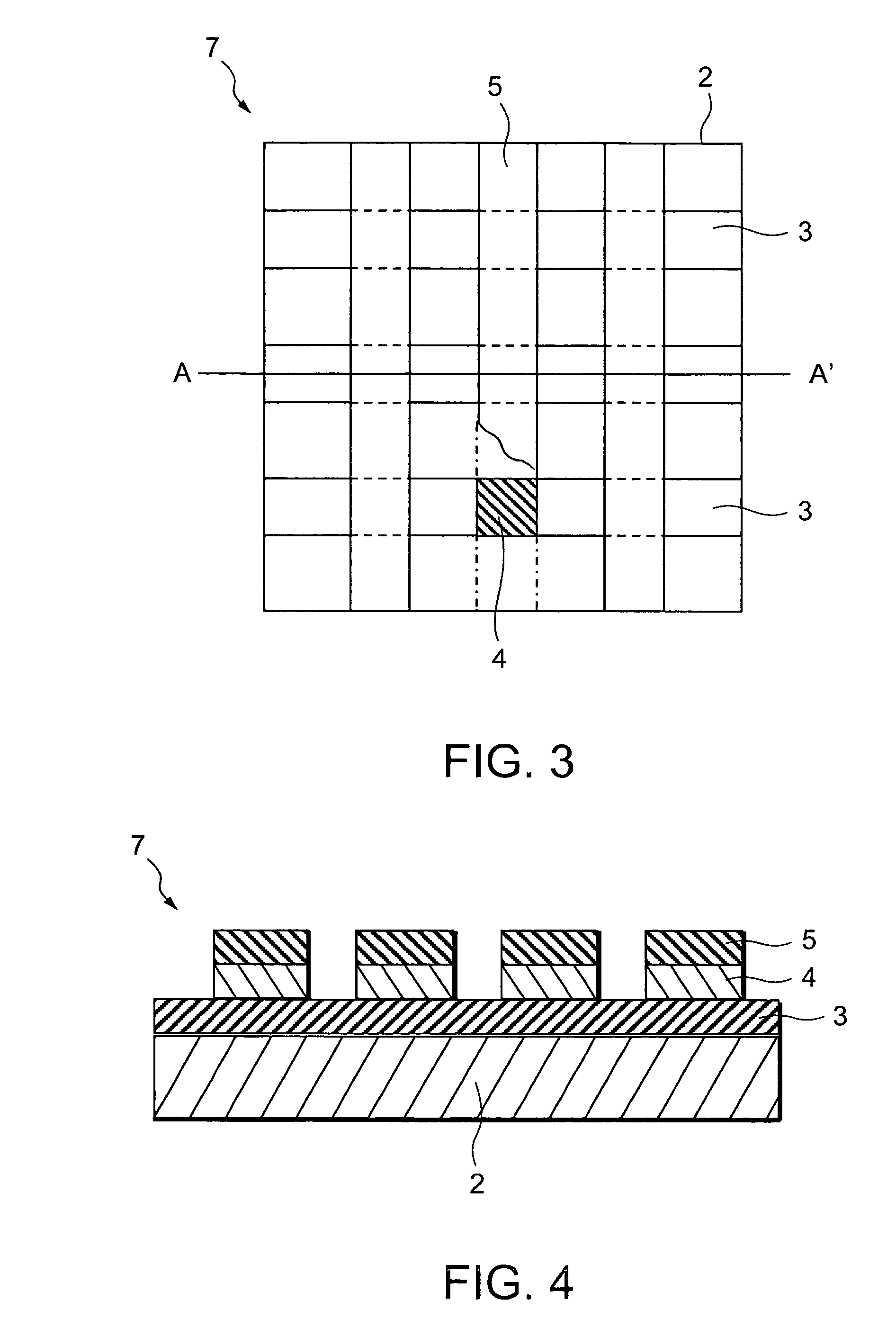
BACKGROUND OF THE INVENTION[0001]1. Field of the Invention[0002]The present invention relates to an organic bistable element, which has a relatively simple structure and can be operated at a low drive voltage, a memory device using the same, and a method for driving the organic bistable element and the memory device.[0003]2. Background Art[0004]A conventional organic bistable element has a laminate structure in which a ferroelectric layer is interposed between a pair of electrodes. For example, anthracene and TTF-CA (an alternately laminated charge transfer complex of tetrathiafulvalene and tetrachloro-p-benzoquinone) have been studied for use as compounds for constituting the ferroelectric layer (see, for example, Japanese Patent Laid-Open No. 345431 / 2001 on pages 2 and 3, FIG. 1).[0005]Further, an organic bistable element has also been proposed in which a laminate having a three-layer structure comprising an electrically conductive thin film interposed between two layers of low-el...
Claims
Login to View More Application Information
Patent Timeline
 IPC IPC(8): B32B9/00H01L51/00G11C13/02
CPCB82Y10/00G11C13/0014Y10T428/31504
InventorKANO, MASATAKA
OwnerDAI NIPPON PRINTING CO LTD