
Power switching circuit
a power switching circuit and circuit technology, applied in the direction of electronic switching, emergency protective arrangements for limiting excess voltage/current, pulse techniques, etc., can solve the problem of possible protection of the power switching circuit, and achieve the effect of accurate avoiding the situation
Patent Information
- Authority / Receiving Office
- US · United States
- Patent Type
- Patents(United States)
- Current Assignee / Owner
- Publication Date
- 2012-12-04
- Estimated Expiration
- Not applicable · inactive patent
Smart Images
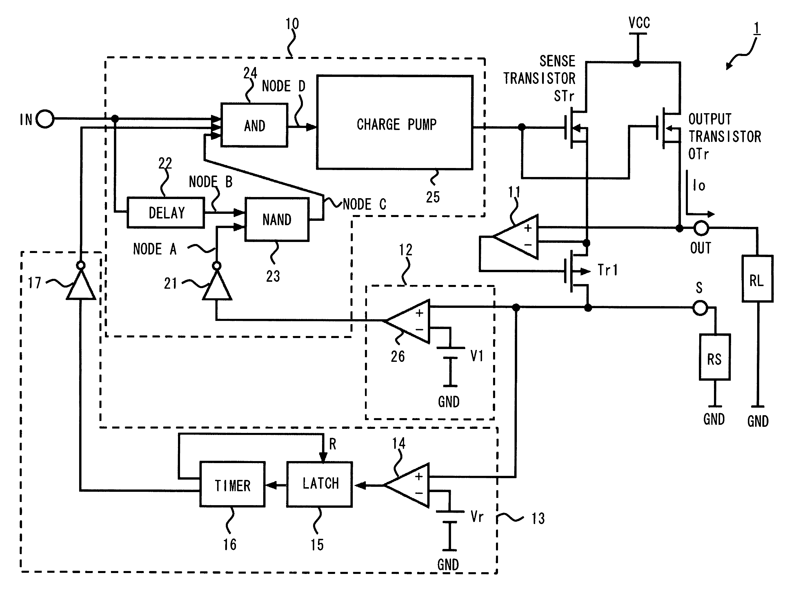
Figure 1 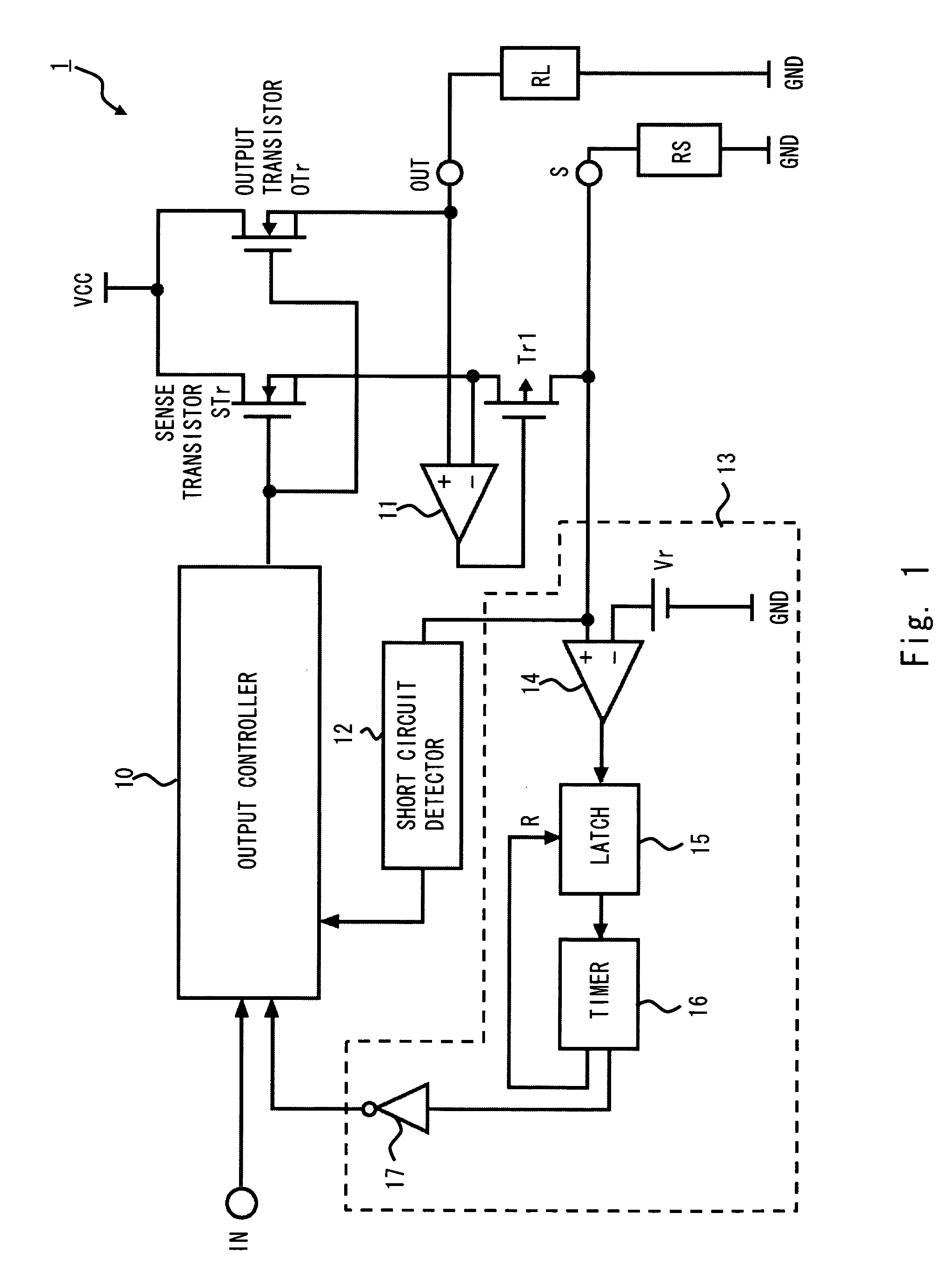
Figure 2 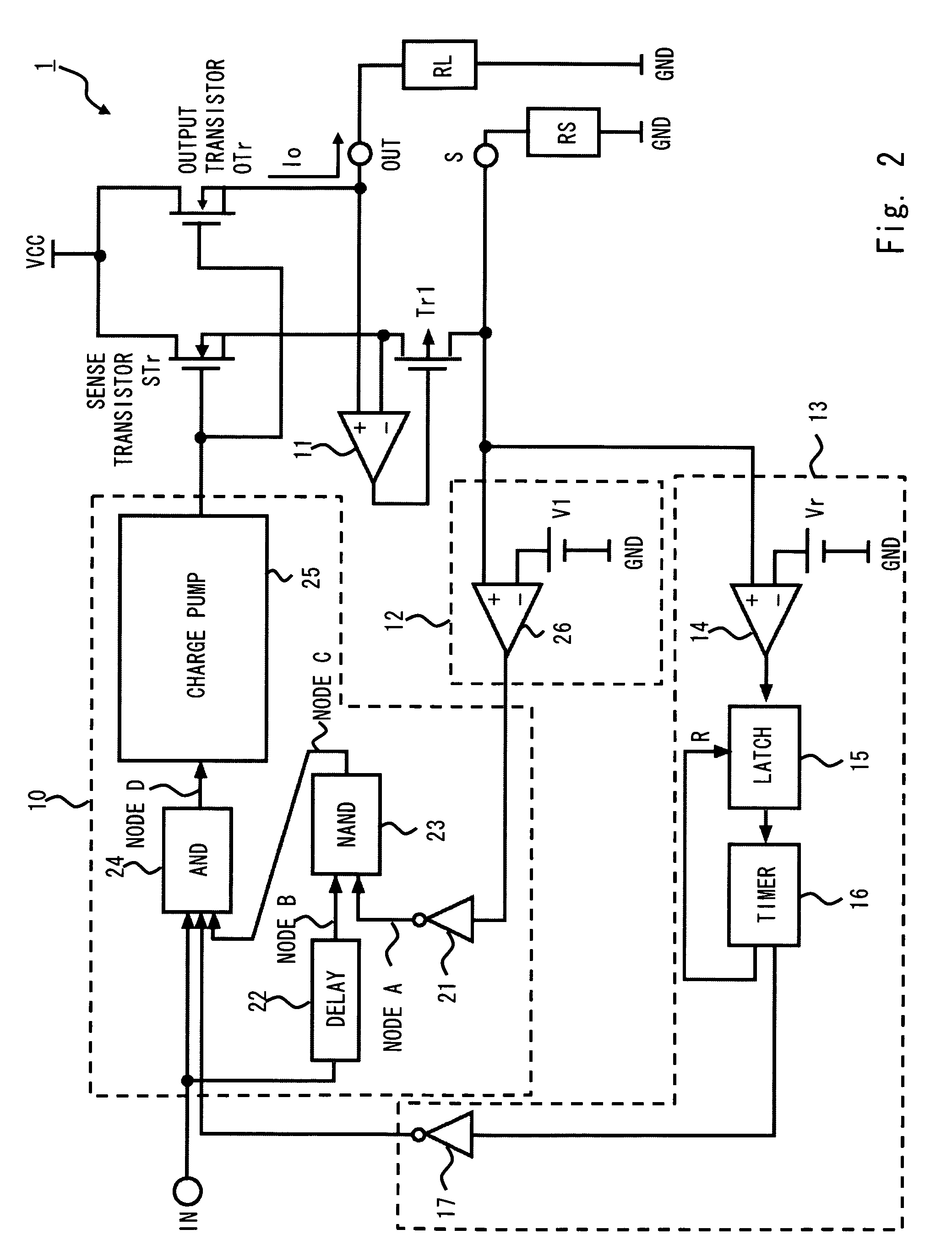
Figure 3
Abstract
Description
BACKGROUND
[0001] 1. Field of the Invention
[0002] The present invention relates to a power switching circuit including an output current detection terminal for detecting an output current that flows into an output transistor.
[0003] 2. Description of Related Art
[0004] Power supply switching circuits mounted between a power supply and a load circuit are often used for controlling a current flowing from the power supply into the load circuit in order to reduce the power consumption of the system. In a power switching circuit, generally an output transistor is connected between a power supply and a load circuit. Then, by operating the output transistor as a switch, the current flowing from the power supply into the load circuit is controlled.
[0005] In such a power switching circuit, if an overcurrent flows into the output transistor due to a defect in the load circuit, a protection system is mounted for detecting the current and reducing or blocking an output current so as to protect the powe...
Examples
first exemplary embodiment
[0033]An exemplary embodiment of the present invention is described hereinafter with reference to the drawings. The block diagram of a power switching circuit 1 according to this embodiment is shown in FIG. 1. As shown in FIG. 1, the power switching circuit 1 includes an output controller 10, an amplifier 11, a short circuit detector 12, an overcurrent detector 13, a transistor Tr1, a sense transistor STr, an output transistor OTr, an input terminal IN, an output terminal OUT and an output current detection terminal S. Moreover, a load RL, which is a load circuit, is connected between the output terminal OUT and a ground terminal GND. A current sense resistor RS is connected between the output current detection terminal S and the ground terminal GND.
[0034]The output controller 10 outputs an output control signal which controls the conducting state of the output transistor OTr according to an input signal input via the input terminal IN. Moreover, when receiving an overcurrent detect...
second exemplary embodiment
[0052]The second exemplary embodiment is another aspect of the output controller 10 and the short circuit detector 12 of the first exemplary embodiment. In the second exemplary embodiment, the power switching circuit includes an output controller 10a and a short circuit detector 12a, which have different aspects from the output controller 10 and the short circuit detector 12. The block diagram of a power switching circuit 2 according to the second exemplary embodiment is shown in FIG. 5.
[0053]The output controller 10a includes an AND circuit 24 and a charge pump circuit 25. The AND circuit 24 outputs an AND operation result of an input signal which is input from the input terminal IN and an overcurrent detection signal which is output by the overcurrent detector 13 to the charge pump circuit 25 as an enable signal. The charge pump circuit 25 outputs an output control signal according to the state of the enable signal as with the first exemplary embodiment.
[0054]The short circuit det...
third exemplary embodiment
[0062]The third exemplary embodiment shows another aspect of the output controller 10 and the short circuit detector 12 of the first exemplary embodiment. In the third exemplary embodiment, a power switching circuit includes an the output controller 10b and a short circuit detector 12b which have different aspects from the output controller 10 and the short circuit detector 12. The block diagram of a power switching circuit 3 according to the third exemplary embodiment is shown in FIG. 9.
[0063]The output controller 10b includes an AND circuit 24 and a charge pump circuit 25. The AND circuit 24 outputs an AND operation result of an input signal which is input from the input terminal IN, an overcurrent detection signal which is output by the overcurrent detector 13 and a short circuit control signal (node H) which is output by the short circuit detector 12b to the charge pump circuit 25 as an enable signal. The charge pump circuit 25 outputs an output control signal according to the s...