
Imaging lens
A camera lens and lens technology, applied in the direction of optical components, optics, instruments, etc., can solve the problems of image plane changes, high manufacturing sensitivity, etc.
Patent Information
- Authority / Receiving Office
- CN · China
- Patent Type
- Patents(China)
- Current Assignee / Owner
- Publication Date
- 2009-10-28
Smart Images
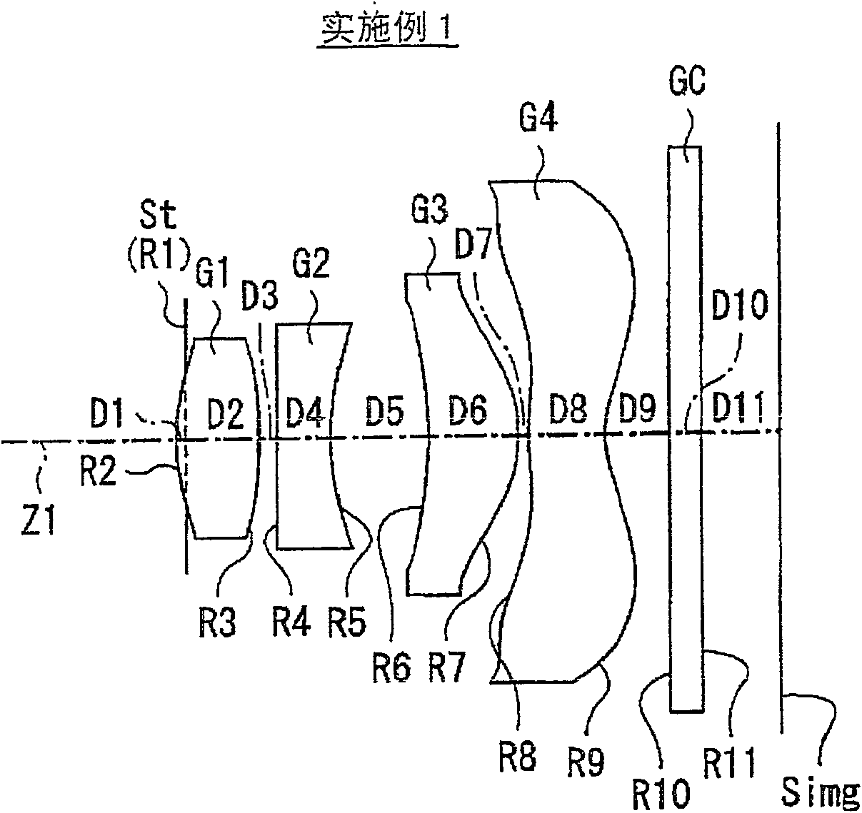
Figure 1 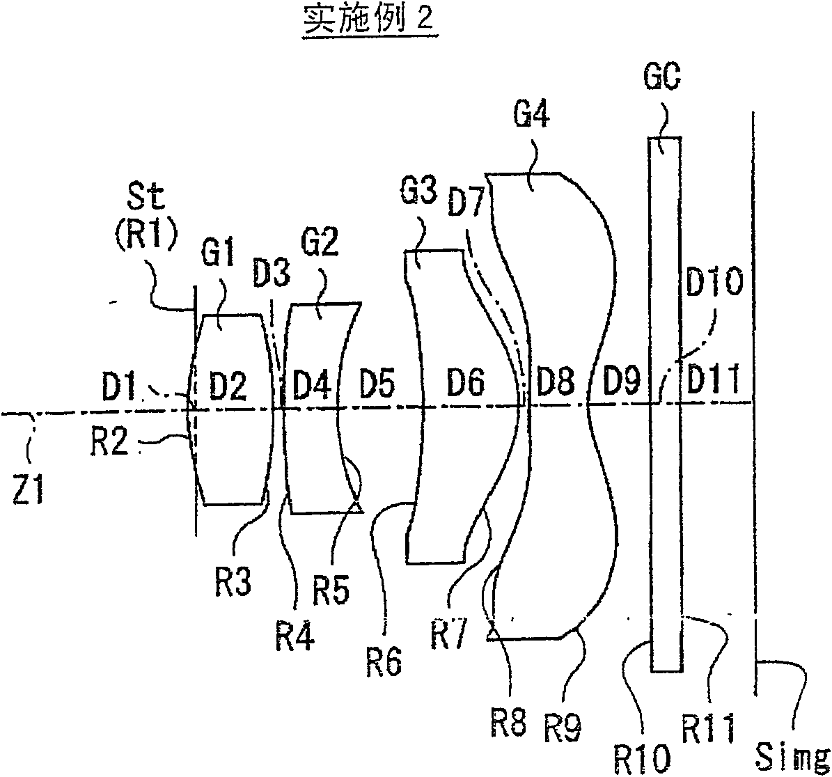
Figure 2 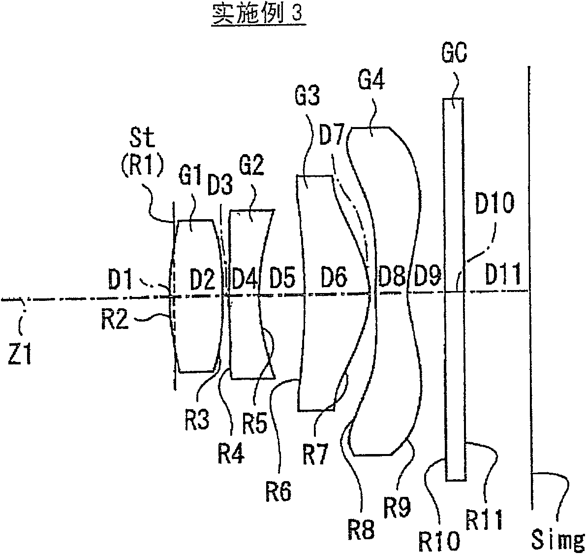
Figure 3
Abstract
Description
technical field
[0001] The present invention relates to an imaging lens mounted on a video camera using an imaging element such as a CCD (Charge Couple Device) or a CMOS (Complementary Metal Oxide Semiconductor). Background technique
[0002] Imaging elements such as CCDs and CMOSs are progressing towards very small size and high speed in recent years. For this reason, small and high-performance devices are also required for the main body of the camera and the lens mounted thereon. In addition, in order to correspond to a high-pixel imaging element, telecentricity is sought, that is, the incident angle to the imaging element is close to parallel to the optical axis (the incident angle to the imaging element is close to perpendicular). Conventionally, most imaging lenses mounted on, for example, a mobile phone with a video camera consist of three lenses, but the number of lenses tends to increase further in order to cope with higher pixel count. Patent Document 1 describe...
Examples
Embodiment 1
[0055] In the imaging lens according to Example 1, both surfaces of the first lens G1 , the second lens G2 , the third lens G3 , and the fourth lens G4 are all aspherical. exist Figure 5 In the basic lens data of (A), as the curvature radii of these aspheric surfaces, the numerical values of the curvature radii near the optical axis are indicated. exist Figure 5 Among the numerical values shown as aspheric data in (B), the symbol "E" indicates that the data immediately following it is a "power exponent" with base 10, indicating that it will be represented by an exponential function with base 10 multiplied by the value before "E". For example, if it is "1.0E-02", it means "1.0×10 -2 ".
[0056] As the aspheric surface data, each coefficient B in the formula representing the aspheric surface shape represented by the following formula (A) i , The value of KA. More specifically, Z represents the length (mm) of a perpendicular line drawn from a point on the aspheric sur...