
RF plasma transparent conductive film
A transparent conductive film, radio frequency plasma technology, applied in the direction of the conductive layer on the insulating carrier, can solve the problems of scattering, affecting the visual effect and light transmittance of the product, and increasing the manufacturing cost, so as to reduce the surface roughness and improve the chemical quality. Composition and wettability, effect of reducing sheet resistance
Patent Information
- Authority / Receiving Office
- CN · China
- Current Assignee / Owner
- Publication Date
- 2011-05-25
- Estimated Expiration
- Not applicable · inactive patent
Smart Images
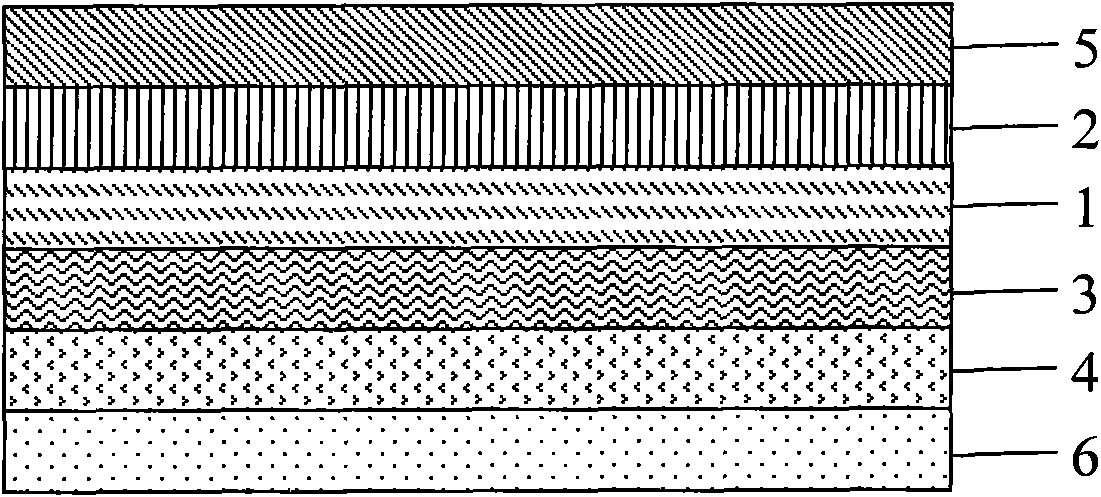
Figure 1 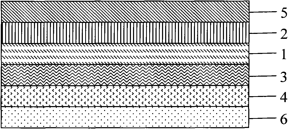
Figure 2
Abstract
Description
technical field
[0001] The invention relates to a conductive composite material, in particular to a transparent conductive film prepared by radio frequency plasma technology. Background technique
[0002] Transparent conductive film is an important material for preparing solar cells, liquid crystal displays and other devices. Transparent conductive film is formed by covering a transparent conductive layer on a transparent substrate. In order to improve the interface adhesion between the substrate and the conductive layer, it is often necessary to A layer of hardened coating is added between the substrate and the transparent conductive layer. The hardened coating needs to be cured under high temperature conditions. However, during the high temperature treatment process, the uneven distribution of molecular structure on the surface of the substrate will cause scattering phenomena, forming " "Rainbow pattern" further affects the visual effect and light transmittance of the prod...
Examples
Embodiment Construction
[0013] Such as figure 1 As shown, the transparent conductive film of radio frequency plasma, the substrate is PET film 1, the front of PET film 1 is coated with hard coating 2, and the surface of hard coating 2 is covered with PE protective film 5; The back of PET film 1 is treated with radio frequency plasma An RF plasma treatment layer 3 is formed, a transparent conductive layer 4 is sputtered on the RF plasma treatment layer 3 , and a PE protective film 6 is covered on the transparent conductive layer 4 .
[0014] The light transmittance of the PET film 1 is above 90%, the dielectric strength is 16.9KV / mm, can block ultraviolet rays, and has low gas and water vapor permeability. The front of the PET film is coated with a hardened coating, and the surface of the hardened coating is covered with a PE protective film; the surface hardness of the hardened coating 2 after hardening reaches more than 3H / 750g, and the light transmittance is > 90%. The hardening process of the hard...