
A kind of reverse polarity algainp base light-emitting diode and its manufacturing method
A technology of light-emitting diodes and manufacturing methods, which is applied in the field of optoelectronics, can solve problems affecting product quality and genuine product rate, poor metal layer adhesion, device voltage increase, etc., to improve quality and yield, improve adhesion and integrity, The effect of the integrity of the electrode structure
Patent Information
- Authority / Receiving Office
- CN · China
- Patent Type
- Patents(China)
- Current Assignee / Owner
- Publication Date
- 2017-05-03
Smart Images
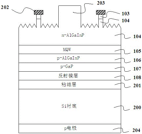
Figure 1 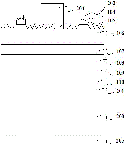
Figure 2 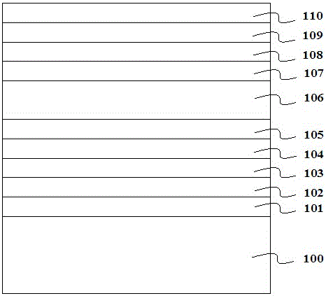
Figure 3
Abstract
Description
Technical field
[0001] The invention belongs to the field of optoelectronic technology, especially the manufacturing technology of reverse polarity AlGaInP-based light-emitting diodes. Background technique
[0002] High-brightness AlGaInP light-emitting diodes have been widely used in high-efficiency solid-state lighting fields, such as display screens, automotive lights, backlights, traffic lights, landscape lighting, etc. Since the forbidden band width of the conventional GaAs substrate is narrower than that of AlGaInP, the photons emitted downward from the active region will be absorbed, resulting in a significant reduction in luminous efficiency. In order to prevent the photons emitted downward from being absorbed and improve the luminous efficiency, a GaP substrate with a wider band gap than AlGaInP can be used to replace the GaAs substrate. However, this process technology has the disadvantages of complicated equipment, low yield, and high manufacturing cost. In view of th...
Examples
Embodiment Construction
[0025] The present invention will be further described below in conjunction with the drawings and embodiments.
[0026] Such as figure 2 As shown, the present invention uses a Si substrate 200 as a permanent substrate and has two main surfaces, an upper and a lower surface. Metal Au or Ag is formed on the upper surface of the adhesive layer 201. The mirror layer 110 is formed on the bonding layer 201, and its material is a SiO2 / Ag double-layer structure; the p-GaP window layer 109 is formed on the mirror layer 110; the p-AlGaInP confinement layer 108 is formed on the p-GaP window On the layer 109; the multiple quantum well (MQW) active layer 107 is formed on the p-AlGaInP confinement layer 108, the material of which is AlGaInP; the n-AlGaInP confinement layer 106 is formed on the multiple quantum well (MQW) active layer 107 On; the n-GaAs ohmic contact layer 105 is formed on the n-AlGaInP confinement layer 106, and its thickness is preferably 300 angstroms, and the doping conc...