
White light LED wafer packaging structure and packaging method
A chip packaging, white light technology, applied in electrical components, electric solid state devices, circuits, etc., can solve the problem of reducing the overall brightness of the product, and achieve the effect of reducing loss, improving light output, and solving the problem of light spots
Patent Information
- Authority / Receiving Office
- CN · China
- Patent Type
- Applications(China)
- Current Assignee / Owner
- Publication Date
- 2016-03-23
- Estimated Expiration
- Not applicable · inactive patent
Smart Images
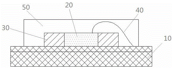
Figure 1 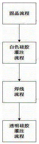
Figure 2
Abstract
Description
technical field
[0001] The invention relates to the technical field of LED packaging, in particular to a white LED chip packaging structure and packaging method. Background technique
[0002] With the continuous development of LED technology, white LED light source devices are widely used in display LED backlight, lighting source and automotive lighting and other fields.
[0003] The existing white light LED light source mainly adopts blue light LED chips to be coated with fluorescent glue around the periphery, and the blue light excites the phosphor powder to mix light to form white light. For products packaged by this process, due to the uneven excitation of the phosphor powder, the light color of the light source is uneven, and it is easy to form a "yellow circle" phenomenon of light spots. As customers have higher and higher requirements for light source quality, it is necessary to completely solve the "yellow circle" phenomenon of light spots. At present, the best solu...
Examples
Embodiment Construction
[0025] Below in conjunction with accompanying drawing, technical scheme of the present invention is described in further detail:
[0026] Such as figure 1 Shown is the LED packaging structure of the present invention, a schematic cross-sectional view of a specific embodiment, specifically including: a substrate 10 , a white LED chip 20 , a white silica gel layer 30 , gold wires 40 and a transparent silica gel layer 50 . The white LED chip is fixed on the substrate, the white silica gel layer is arranged on the side of the white LED chip, the white LED chip and the substrate are connected by gold wires, and the transparent silica gel layer is coated on the white LED chip and the white silica gel layer.
[0027] The substrate 10 is a ceramic substrate or a metal substrate with high thermal conductivity. The substrate 10 makes the LED packaging structure have good heat dissipation and stable and reliable quality.
[0028] The white LED chip 20 is a vertical structure chip. Usin...