
4H-SiC metal semiconductor field effect transistor having double high gates
A field-effect transistor and metal-semiconductor technology, which is applied in the field of 4H-SiC metal-semiconductor field-effect transistors, can solve the problems that the saturation leakage current has not been substantially improved, the effective mobility of carriers has decreased, and the saturation current has degraded, etc. Maximum output power density, increase in breakdown voltage, and the effect of increasing breakdown voltage
Patent Information
- Authority / Receiving Office
- CN · China
- Current Assignee / Owner
- Publication Date
- 2016-09-07
Smart Images
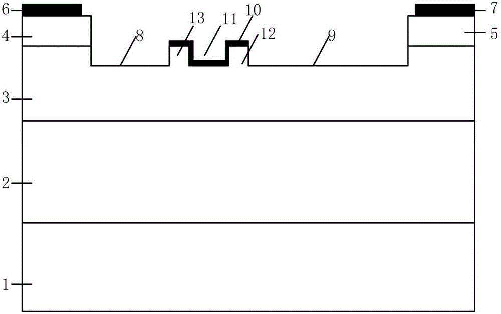
Figure 1
Abstract
Description
technical field
[0001] The invention belongs to the technical field of field effect transistors, in particular to a 4H-SiC metal semiconductor field effect transistor with double high gates. Background technique
[0002] SiC materials have outstanding material and electrical properties such as wide band gap, high breakdown electric field, high saturated electron migration velocity, and high thermal conductivity, making them suitable for high-frequency and high-power device applications, especially high temperature, high voltage, aerospace, satellite, etc. It has great potential in high-frequency high-power device applications in harsh environments. In SiC allomorphs, the electron mobility of 4H-SiC with hexagonal close-packed wurtzite structure is nearly three times that of 6H-SiC, so 4H-SiC materials are used in high-frequency and high-power devices, especially in metal-semiconductor fields. Effect transistor (MESFET) occupies a major position in the application.
[0003] ...
Examples
Embodiment Construction
[0018] The present invention will be further described below in conjunction with the embodiments and with reference to the accompanying drawings.
[0019] See figure 1 .
[0020] A 4H-SiC metal-semiconductor field-effect transistor with a double-high gate, including a 4H-SiC semi-insulating substrate 1, a P-type buffer layer 2, an N-type channel layer 3, and an N-type channel layer 3 from bottom to top On both sides are the source cap layer 4 and the drain cap layer 5 respectively, the surfaces of the source cap layer 4 and the drain cap layer 5 are the source electrode 6 and the drain electrode 7 respectively, above the N-type channel layer 3 and close to the source cap A gate electrode 10 is formed on one side of the layer, and the gate electrode 10 forms a left channel recessed area 8, a right channel recessed area 9, and a middle channel recessed area 11 on the left, right, and middle of the N-type channel 3, respectively. A left upper gate region 13 and a right upper ga...