
4h-sic metal-semiconductor field-effect transistor with stepped buffer layer structure
A field-effect transistor and metal-semiconductor technology, which is applied in the field of 4H-SiC metal-semiconductor field-effect transistors, can solve problems such as no increase in saturation leakage current, lattice damage, and reduced drain current.
Patent Information
- Authority / Receiving Office
- CN · China
- Patent Type
- Patents(China)
- Current Assignee / Owner
- Publication Date
- 2017-06-30
Smart Images
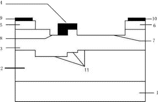
Figure 1 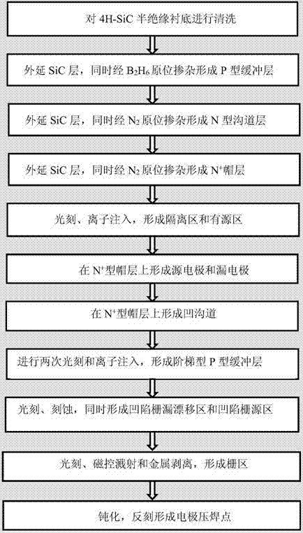
Figure 2
Abstract
Description
technical field
[0001] The invention relates to the technical field of field effect transistors, in particular to a 4H-SiC metal semiconductor field effect transistor with a ladder buffer layer structure. Background technique
[0002] SiC materials have outstanding material and electrical properties such as wide band gap, high breakdown electric field, high saturated electron migration velocity, and high thermal conductivity, making them suitable for high-frequency and high-power device applications, especially high temperature, high voltage, aerospace, satellite, etc. It has great potential in high-frequency high-power device applications in harsh environments. In SiC allomorphs, the electron mobility of 4H-SiC with hexagonal close-packed wurtzite structure is nearly three times that of 6H-SiC, so 4H-SiC materials are used in high-frequency and high-power devices, especially in metal-semiconductor fields. Effect transistor (MESFET) occupies a major position in the applicat...
Examples
Embodiment 1
[0031] Example 1: Fabricate a 4H-SiC metal-semiconductor field-effect transistor with a thickness of 0.53 μm and a stepped P-type buffer layer with two steps 11 of 0.03 μm and 0.05 μm.
[0032] The manufacturing steps of this embodiment are as follows:
[0033] Step 1: cleaning the 4H-SiC semi-insulating substrate 1 to remove surface pollutants.
[0034] (1.1) Carefully wash the substrate twice with a cotton ball dipped in methanol to remove SiC particles of various sizes on the surface;
[0035] (1.2) Place 4H-SiC semi-insulating substrate 1 in H 2 SO 4 :HNO 3 = Ultrasound for 5 minutes in 1:1;
[0036] (1.3) Put 4H-SiC semi-insulating substrate 1 in 1# cleaning solution (NaOH:H 2 o 2 :H 2 O=1:2:5), boiled for 5 minutes, rinsed with deionized water for 5 minutes, and then put into 2# cleaning solution (HCl:H 2 o 2 :H 2 O=1:2:7) and boiled for 5 minutes. Finally rinsed with deionized water and rinsed with N 2 Blow dry and set aside.
[0037] Step 2: Epitaxially gr...
Embodiment 2
[0077] Embodiment 2: Fabricate a 4H-SiC metal-semiconductor field-effect transistor with a thickness of 0.52 μm and a stepped P-type buffer layer with two steps of 0.03 μm and 0.03 μm. In the manufacturing steps of this embodiment:
[0078] Step 2: Epitaxially grow a SiC layer on the surface of the 4H-SiC semi-insulating substrate 1, while diborane B 2 h 6 In-situ doping forms the P-type buffer layer 2 .
[0079] Put the 4H-SiC semi-insulating substrate 1 into the growth chamber, and feed silane with a flow rate of 20ml / min, propane with a flow rate of 10ml / min and high-purity hydrogen with a flow rate of 80l / min into the growth chamber, and simultaneously feed 2ml / min of B 2 h 6 (H 2 diluted to 5%), the growth temperature was 1550°C, and the pressure was 10 5 Pa, last for 6min, complete doping concentration and thickness are 1.4×10 15 cm -3 and a P-type buffer layer 2 of 0.52 μm.
[0080] Step 3: epitaxially grow the SiC layer on the P-type buffer layer 2, and at the ...
Embodiment 3
[0089] Embodiment 3: Fabricate a 4H-SiC metal-semiconductor field-effect transistor with a thickness of 0.55 μm and a stepped P-type buffer layer with two steps of 0.05 and 0.05 μm. In the manufacturing steps of this embodiment:
[0090] Step 2: Epitaxial growth of SiC layer on the surface of 4H-SiC semi-insulating substrate, while diborane B 2 h 6 In-situ doping forms a P-type buffer layer.
[0091] Put the 4H-SiC semi-insulating substrate 1 into the growth chamber, and feed silane with a flow rate of 20ml / min, propane with a flow rate of 10ml / min and high-purity hydrogen with a flow rate of 80l / min into the growth chamber, and simultaneously feed 2ml / min of B 2 h 6 (H 2 diluted to 5%), the growth temperature was 1550°C, and the pressure was 10 5 Pa, last for 6min, complete doping concentration and thickness are 1.4×10 15 cm -3 and a P-type buffer layer 2 of 0.55 μm.
[0092] Step 3: epitaxially grow the SiC layer on the P-type buffer layer 2, and at the same time 2 ...