
A kind of lateral structure impatt diode and preparation method thereof
A lateral structure, diode technology, applied in diodes, semiconductor/solid-state device manufacturing, semiconductor devices, etc., can solve the problems that restrict the performance of traditional vertical structure IMPATT, difficult metal-P-type GaN barrier height, and difficult to form high-quality P-type ohmic contact and other problems, to achieve the effect of enhancing low field mobility, significant negative differential mobility effect, and reducing device size
Patent Information
- Authority / Receiving Office
- CN · China
- Patent Type
- Patents(China)
- Current Assignee / Owner
- Publication Date
- 2021-04-30
Smart Images
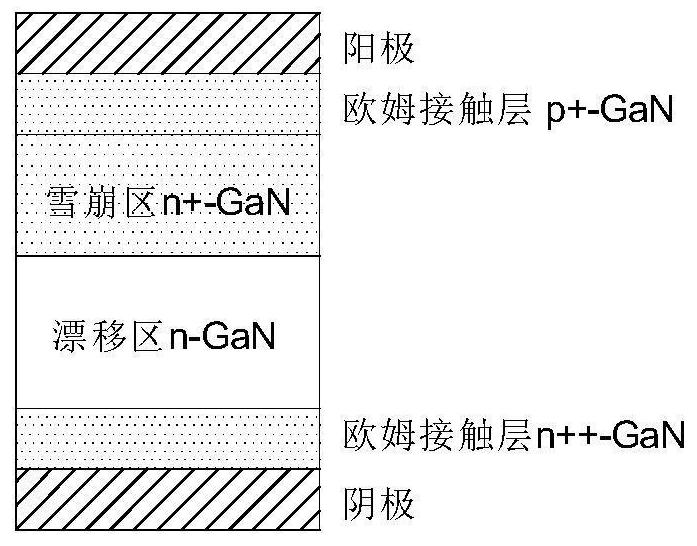
Figure 1 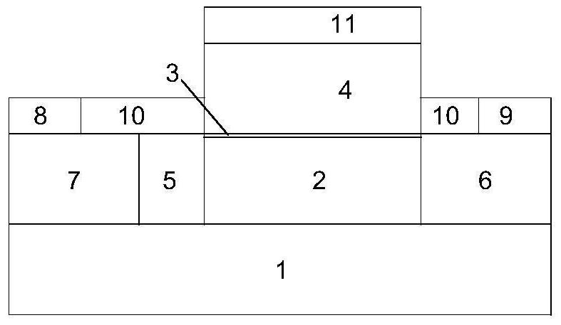
Figure 2 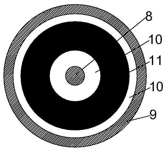
Figure 3
Abstract
Description
technical field
[0001] The invention belongs to the technical field of semiconductors, and relates to a lateral structure IMPATT diode and a preparation method thereof. Background technique
[0002] Avalanche diode (IMPATT) is a semiconductor device that uses impact ionization in semiconductors to generate charge packets, and the charge packets pass through to generate negative resistance at a certain frequency. Because avalanche will produce avalanche delay, carriers drifting inside the device through a finite time will produce transit time delay. The superposition of these two delays will cause the establishment of avalanche current to lag behind the terminal voltage, thus generating negative resistance. When the sum of these two delays falls within the range of 1 / 4 cycle to 3 / 4 cycle (90° to 270° phase difference), the dynamic resistance of the diode is negative at this time. As one of the most efficient and powerful microwave solid-state sources, IMPATT diodes have rece...
Examples
Embodiment Construction
[0041] The present invention will be described in further detail below in conjunction with specific examples, but not as a limitation of the present invention.
[0042] refer to figure 2 , the lateral structure IMPATT diode of the present invention comprises a substrate layer 1, an epitaxial layer 2, a drift layer 3, an n-AlGaN barrier layer 4, an n+-GaN barrier layer 5, a right ohmic contact layer 6, a left ohmic contact layer 7, a left Ohmic contact electrode 8 , right ohmic contact electrode 9 , passivation layer 10 , Schottky contact electrode 11 .
[0043] The epitaxial layer 2 is located on the upper layer of the substrate layer 1; the drift layer 3 is a two-dimensional electron gas thin layer formed on the top of the epitaxial layer 2 when electricity is applied; the n-AlGaN barrier layer 4 is located on the upper layer of the drift layer 3; n+-GaN The barrier layer 5 is located on the upper layer of the substrate layer 1 and on the left side of the epitaxial layer 2;...