
Array substrate, manufacturing method thereof and display device
A technology of an array substrate and a manufacturing method, which is applied in the field of display devices, can solve the problems of backlight source occupancy, restricting battery life, etc., and achieve the effects of saving power consumption, improving battery life, and simple manufacturing method.
Patent Information
- Authority / Receiving Office
- CN · China
- Patent Type
- Applications(China)
- Current Assignee / Owner
- Publication Date
- 2021-11-09
Smart Images
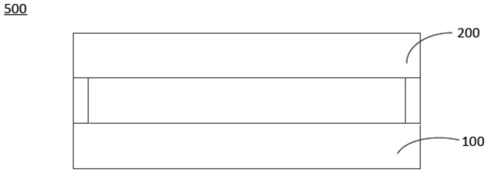
Figure 1 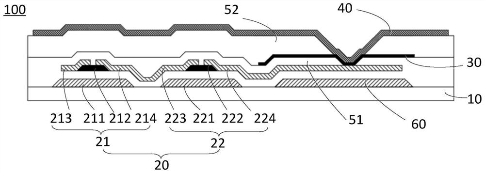
Figure 2 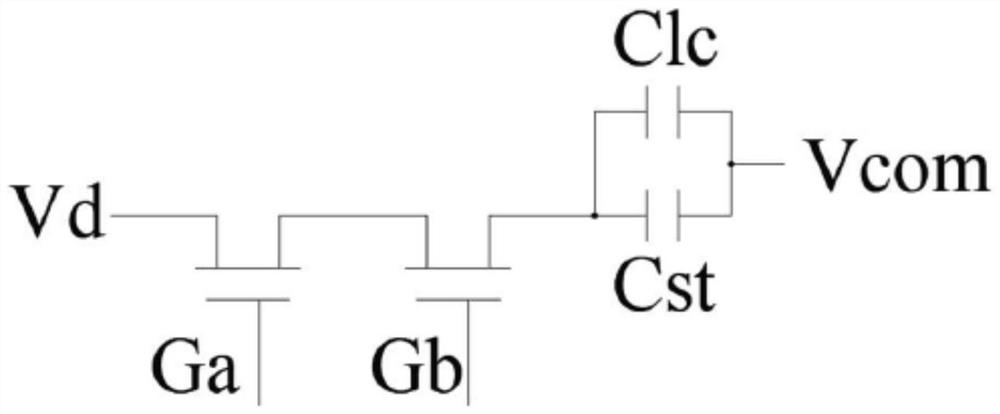
Figure 3
Abstract
Description
technical field
[0001] The present invention relates to the field of display devices, in particular to an array substrate, a manufacturing method thereof, and a display device. Background technique
[0002] A Liquid Crystal Display (LCD) is a display device that presents desired images by selectively transmitting light emitted from a backlight source by utilizing the polarization phenomenon of liquid crystals. TFT is the abbreviation of "Thin Film Transistor", which generally refers to thin film transistor displays. The most common type of TFT LCD is twisted nematic (Twisted Nematic, TN) LCD, which includes an array substrate, a color filter substrate, a liquid crystal (Liquid Crystal) between them, and a backlight. The polarized light is formed by the polarizer on the array substrate, then rotated by 90° through the liquid crystal in the LCD cell, and then transmitted by the polarizer on the color filter substrate to present an image.
[0003] Since TFT-LCD usually requir...
Examples
Embodiment Construction
[0047] In order to make the object, technical solution and advantages of the present invention clearer, the present invention will be further described in detail below in conjunction with the accompanying drawings, that is, embodiments. It should be understood that the specific embodiments described here are only used to explain the present invention, not to limit the present invention.
[0048] It should be noted that when a component is referred to as being “fixed on” or “disposed on” another component, it may be directly or indirectly on the other component. When an element is referred to as being "connected to" another element, it can be directly or indirectly connected to the other element. The orientation or positional relationship indicated by the terms "upper", "lower", "left", "right", etc. are based on the orientation or positional relationship shown in the drawings, and are for convenience of description only, rather than indicating or implying the referred device ...