
Gallium oxide nanostructure device, and production method and application thereof
A nanostructure, gallium oxide technology, applied in the direction of nanotechnology, nanotechnology, nanotechnology for sensing, etc., can solve the problems of weak response-recovery ability, inaccurate resistance measurement, and influence on detection effect, etc. Sensitive performance, overcoming large resistance, and reducing cost
Patent Information
- Authority / Receiving Office
- CN · China
- Patent Type
- Applications(China)
- Current Assignee / Owner
- Publication Date
- 2021-11-26
Smart Images
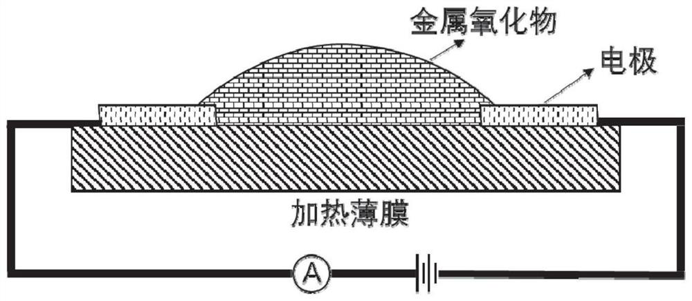
Figure 1 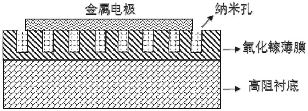
Figure 2 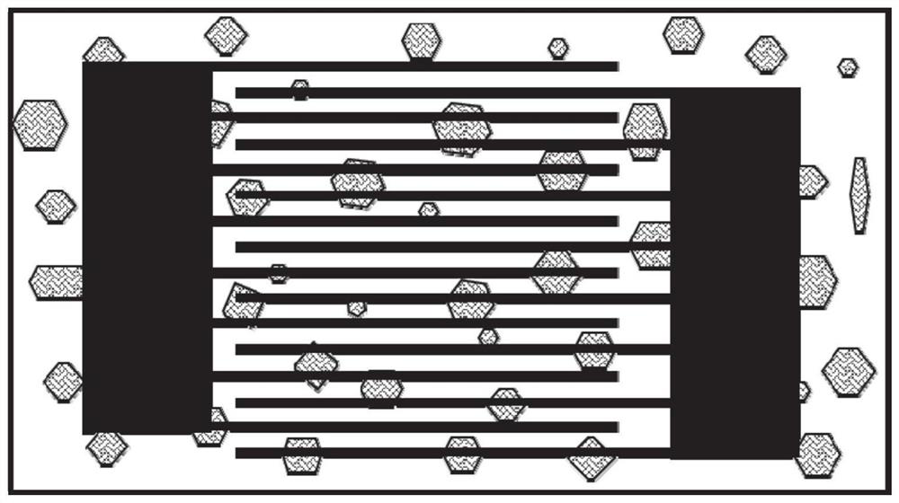
Figure 3
Abstract
Description
technical field
[0001] The invention relates to a thin-film gas sensor, in particular to a gallium oxide nanostructure device and its preparation method and application, belonging to the fields of electronic information and technology and semiconductor technology. Background technique
[0002] In the process of industrialization and urbanization, people pay more and more attention to air pollution caused by automobile exhaust and chemical poisonous gas; especially the gas leakage in industrial production has major safety hazards, so it is very important to effectively detect various toxic and harmful gases . Thin-film metal-oxide-semiconductor gas sensors play an important role in the field of gas detection due to their advantages of high sensitivity, simple fabrication, small size, low price, compatibility with microelectromechanical systems (MEMS) processes, and easy mass production. favored by many researchers. At present, commonly used gas sensing materials are NiO, Sn...
Examples
preparation example Construction
[0077] see image 3 , in a more typical embodiment of the present invention, a preparation method of a gallium oxide nanostructure device may comprise the following steps:
[0078] 1) Epitaxy of gallium oxide thin films: use metal organic compound chemical vapor deposition (MOCVD) or molecular beam epitaxy (MBE) or hydride vapor phase epitaxy (HVPE) on heterogeneous or homogeneous substrates (heterogeneous substrates include but Not limited to sapphire and other materials) to grow gallium oxide thin films, and adjust the n-type doping concentration;
[0079] 2) Metal Ga is etched to form nanopores: Metal organic compound chemical vapor deposition (MOCVD) or molecular beam epitaxy (MBE) or atomic layer deposition (ALD) is used to deposit metal gallium on the surface of gallium oxide film, so that the gallium oxide film Surface corrosion forms a plurality of nanopores of different depths or the same depth; at least one condition in the temperature of deposition, the pressure of...
Embodiment 1
[0088] 1) The metal-organic vapor deposition (MOCVD) process was used to deposit Ga 2 o 3 film growth;
[0089]2) Use high-purity oxygen and triethylgallium (TEGa) as the oxygen source and gallium source respectively, and control the flow rates to 200 sccm and 500 sccm respectively; and use high-purity nitrogen as the carrier gas of TEGa; adjust the temperature in the reaction chamber to 500°C, The pressure is kept at 20KPa, and the growth time is 2 hours to obtain Ga with a thickness of about 10nm-10μm. 2 o 3 film;
[0090] 3) Also use MOCVD equipment to introduce TEGa into the reaction chamber, and control the flow rate of TEGa to 100 sccm, the temperature in the reaction chamber to 500 °C, and pre-deposit Ga droplets on the Ga 2 o 3 On the thin film, the deposition time is 10 minutes; after the pre-deposition is completed, the gallium source supply is stopped, and the temperature in the reaction chamber is raised to 660 °C, Ga droplets and Ga 2 o 3 The film undergoes...