
Thin film semiconductor device and method for manufacturing same
a technology of thin film and semiconductors, applied in the direction of semiconductor devices, electrical devices, transistors, etc., to achieve the effect of reducing the fluctuation of the vth valu
Patent Information
- Authority / Receiving Office
- US · United States
- Patent Type
- Applications(United States)
- Current Assignee / Owner
- Publication Date
- 2005-03-03
- Estimated Expiration
- Not applicable · inactive patent
Smart Images
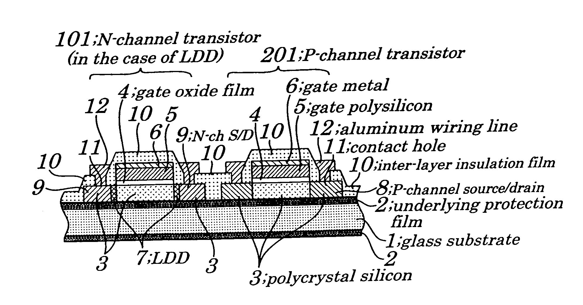
Figure 1 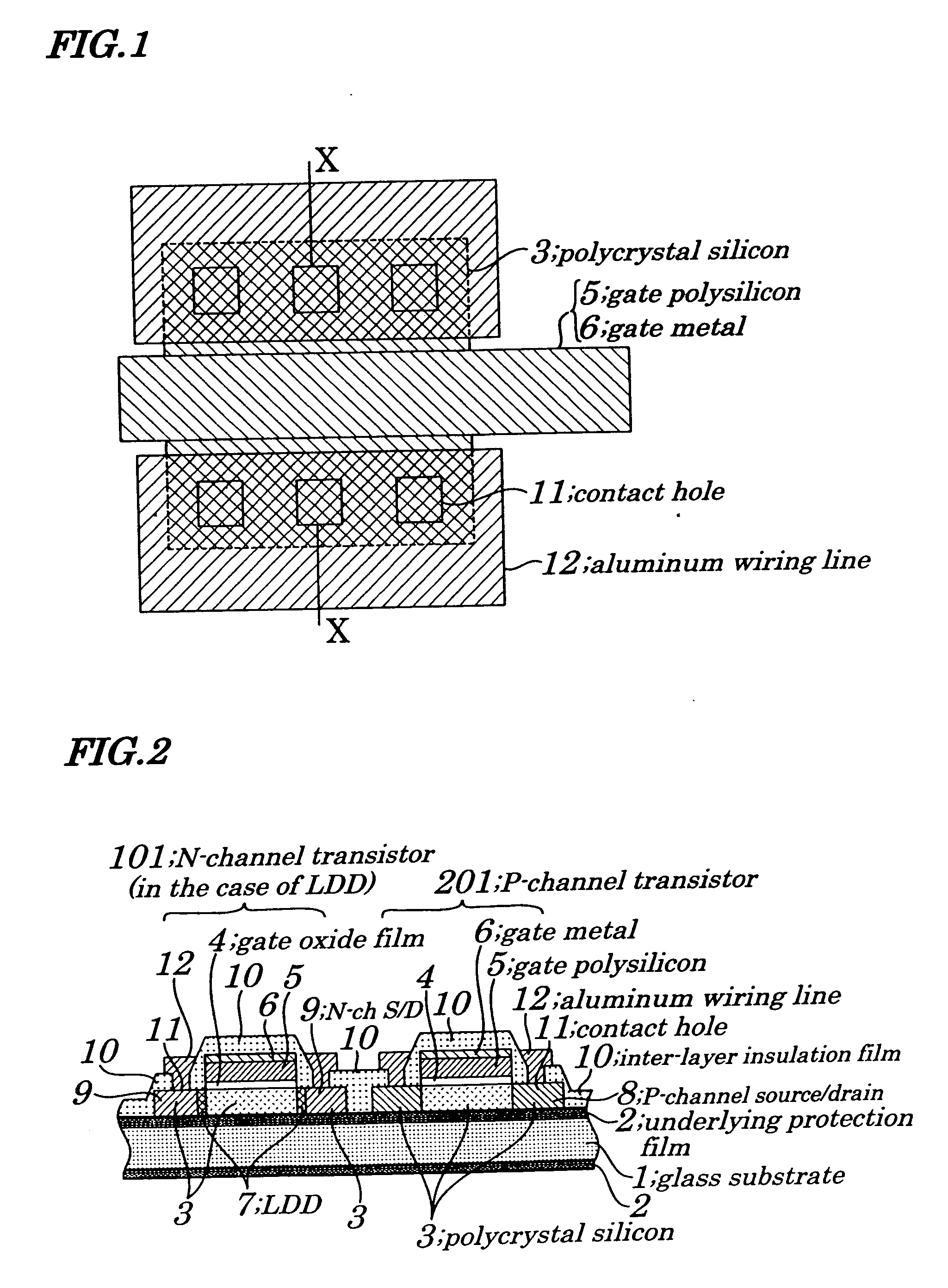
Figure 2 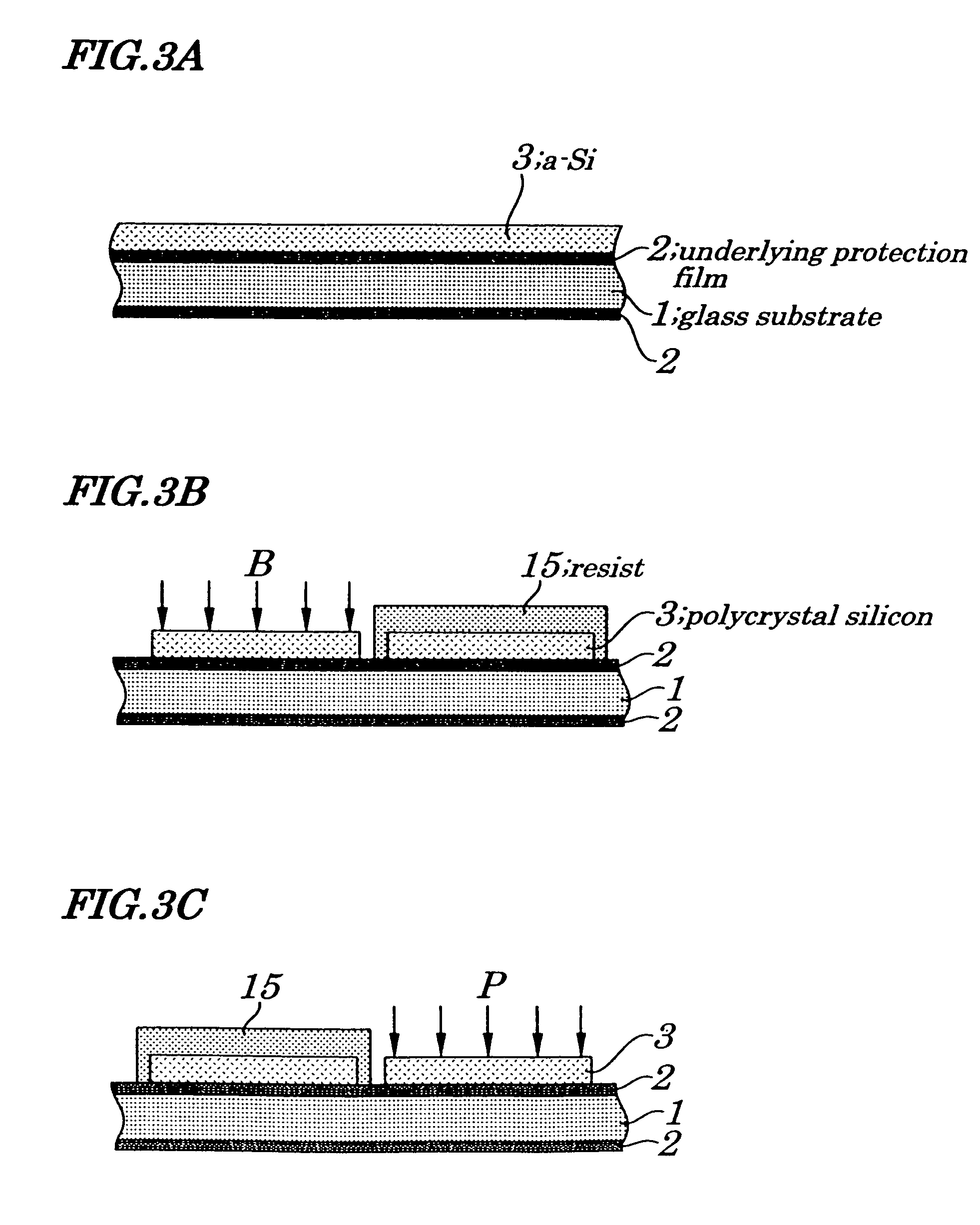
Figure 3
Abstract
Description
BACKGROUND OF THE INVENTION 1. Field of the Invention The present invention relates to a thin film semiconductor device and method for manufacturing the same. The present application claims priority of Japanese Patent Application No. 2002-064795 filed on Mar. 11, 2002, which is hereby incorporated by reference. 2. Description of the Related Art Conventionally, in a CMOS (Complementary Metal Oxide Semiconductor)-type thin film semiconductor device, a gate electrode of an N (negative)-channel transistor and that of a P (positive)-channel transistor have been made of only a single metal material or only a single conductivity-type polysilicon material. By this method, however, a gate electrode material of the N-channel transistor and that of the P-channel transistor have a same work function, so that in order to give almost the same threshold voltage (Vth) to the two transistors, it has been necessary to extremely reduce a channel impurity concentration of either of the gate electr...
Examples
first embodiment
First, a thin film semiconductor device and method for manufacturing the same according to a first embodiment of the present invention is described with reference to FIGS. 1-2 and 3A-3H. Of these, FIGS. 3A-3H show one series of manufacturing steps and are actually divided for convenience of plotting.
The following will describe a thin film semiconductor device manufacturing method according to the first embodiment with reference to FIGS. 3A-3H. First, as shown in FIG. 3A, on a glass substrate 1 is formed an underlying protection film 2 made of SiO2 to a thickness of about 100 nm (1000 Å), on which is formed a-Si 3 by LP-CVD (Low Pressure Chemical Vapor Deposition) or PE-CVD (Plasma-Enhanced Chemical Vapor Deposition) to a thickness of about 60 nm. In the case where PE-CVD (Plasma-Enhanced Chemical Vapor Deposition) is employed in the formation, the a-Si 3 is dehydrogenated to 1% or less before the next step of crystallization by use of excimer laser or a like. Then, the substrate ...
second embodiment
The following will describe a thin film semiconductor device and method for manufacturing the same according to a second embodiment of the present invention, with reference to FIGS. 4A-4D. FIGS. 4A-4D are actually divided for convenience of plotting. In contrast to the above-mentioned first embodiment in which the present invention is applied to an LDD (Lightly Doped Drain) construction using a photo-resist process, the present embodiment applies the present invention to an LDD construction employing a self-alignment (SA) to hereby enable reducing the time required by the steps.
The method for manufacturing the thin film semiconductor device having this construction is shown in FIGS. 4A-4D. In these figures, the present embodiment uses the same steps as those of the first embodiment up to the growing of a gate oxide film 4. After that, as shown in FIG. 4A, gate polysilicon 5 is grown to a thickness of about 60 nm. Preferably the gate polysilicon 5 is formed roughly as thick as a t...
third embodiment
The following will describe a thin film semiconductor device and method for manufacturing the same according to a third embodiment of the present invention, with reference to FIGS. 5A-5C. In contrast to the above-mentioned second embodiment in which the present invention is applied to an LDD (Lightly Doped Drain) construction using SA (Self-Alignment), the present invention may be applied to an LDD construction using a side wall in the present embodiment.
The manufacturing method is described below with reference to FIGS. 5A-5C. In the figures, the present embodiment uses the same steps as those of the second embodiment up to the patterning of a gate polysilicon 5 making up a gate electrode through a gate dry etching process. After the gate electrode is patterned, a P-channel transistor's LDD is selectively formed (see FIG. 5A) by performing a lightly doped drain photo-resist process for Boron (B) doping and a subsequent boron (B) ion injection process (see FIG. 5A) and then an N-...