
Electro-optical device, manufacturing method of the same, and electronic apparatus
Patent Information
- Authority / Receiving Office
- US · United States
- Current Assignee / Owner
- Publication Date
- 2005-04-21
Smart Images
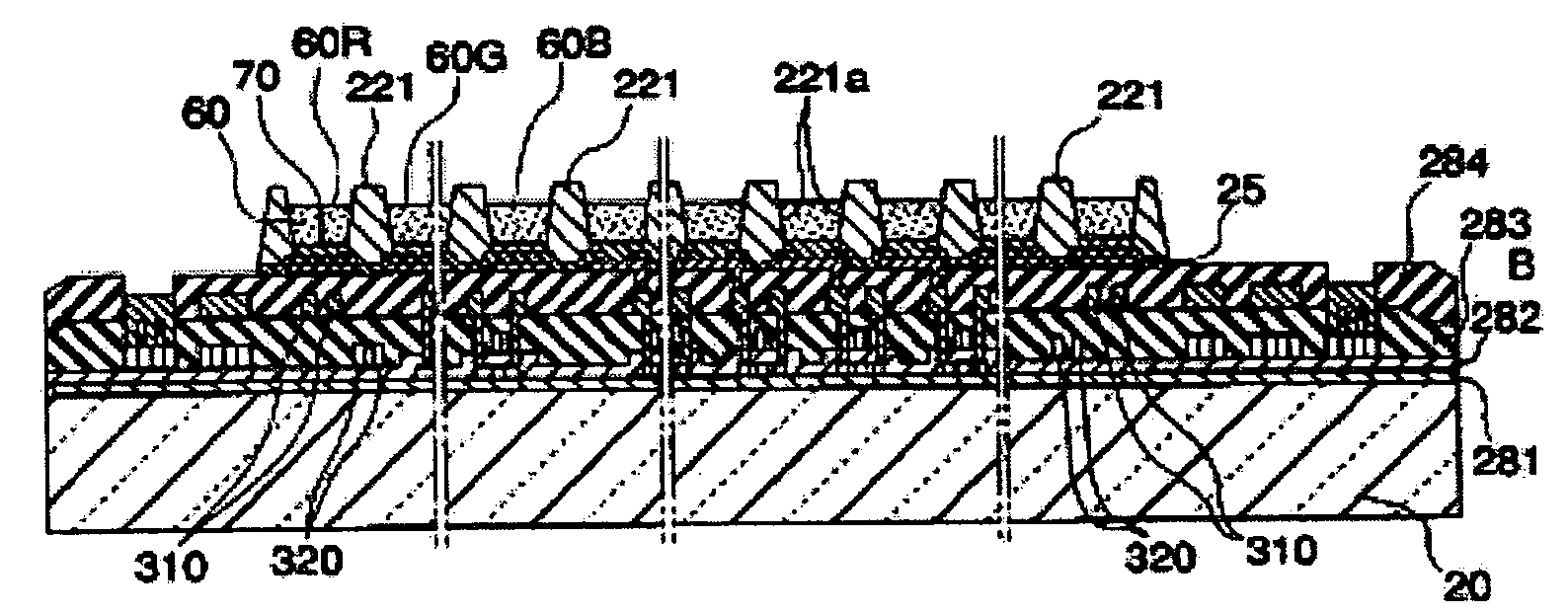
Figure 1 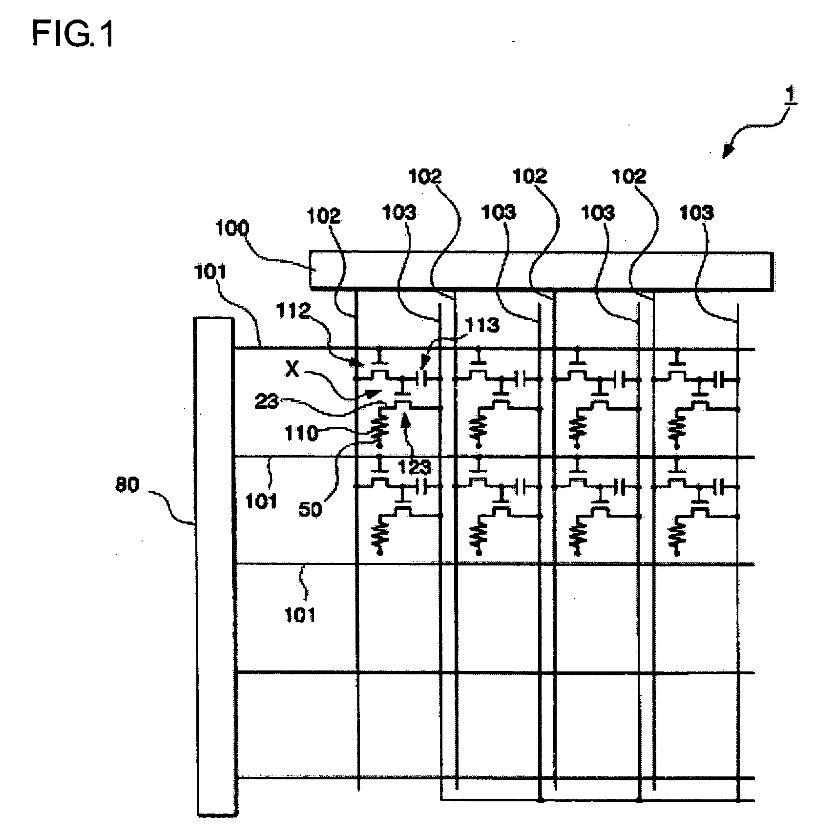
Figure 2 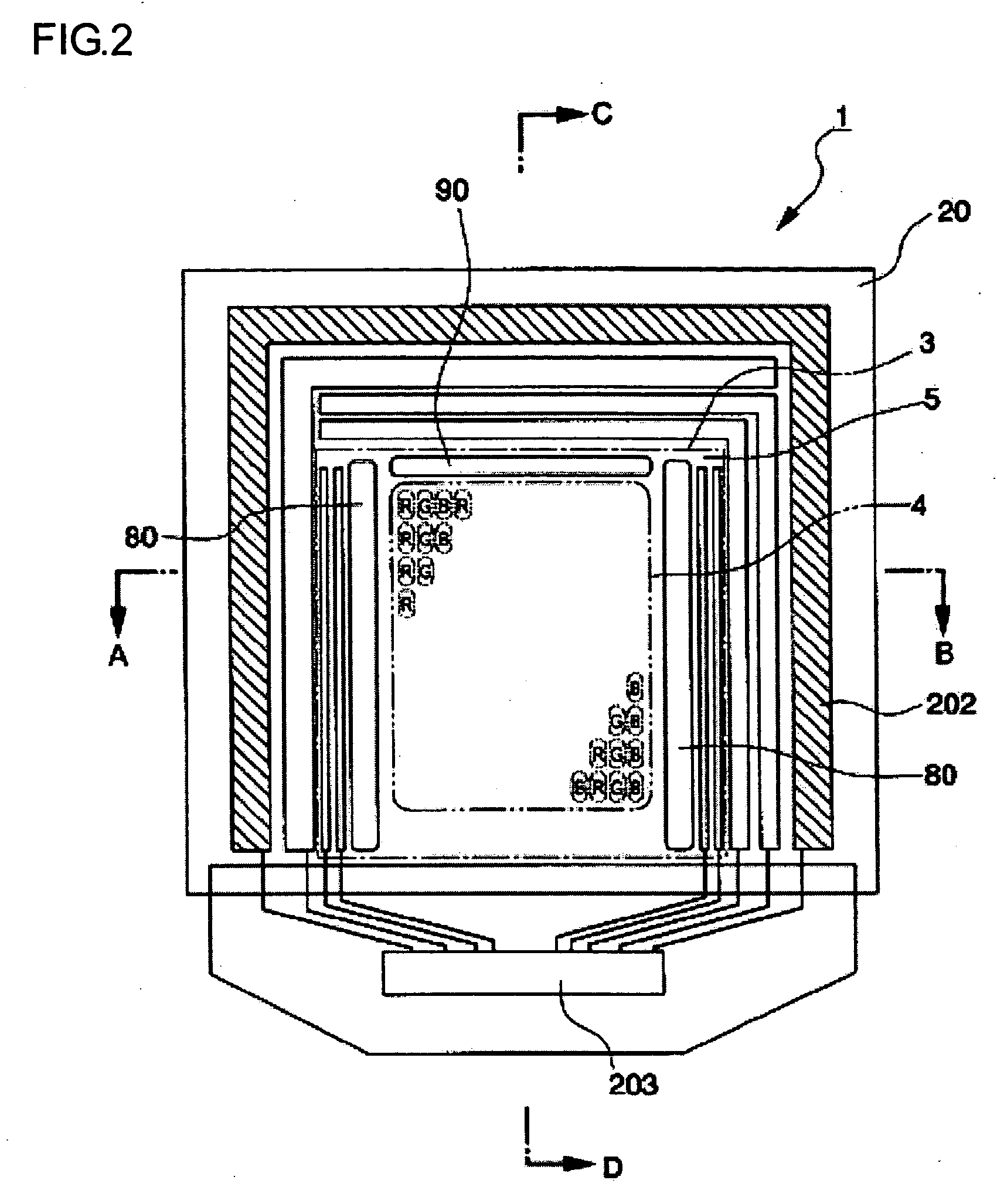
Figure 3
Abstract
Description
BACKGROUND OF THE INVENTION
[0001] 1. Field of Invention
[0002] The present invention relates to an electro-optical device, a manufacturing method of the same, and an electronic apparatus equipped with the electro-optical device.
[0003] 2. Description of Related Art
[0004] It has been one of the subjects in the field of electro-optical devices to enhance the durability of the devices against oxygen, water, and so forth. For example, in organic electroluminescence (hereinafter, abbreviated to organic EL) display devices, which are examples of the electro-optical devices, electro-optical materials (organic EL materials, hole-injection materials, electron-injection materials, or the like) for forming light-emitting layers (electro-optical layers) are deteriorated due to oxygen, water, or the like, and the conductivity of cathodes are reduced due to oxygen, water or the like, and thus, non-light-emitting regions called dark spots are formed. Therefore, problems occur in that the service...
Examples
Embodiment Construction
[0044] Hereinafter, embodiments of the electro-optical device, the method of producing the same, and the electronic apparatus of the present invention will be described with reference to the drawings.
[0045] As the electro-optical device, an EL display device using a field light-emissive substance, especially, an organic electroluminescence (EL) material will be described.
[0046]FIG. 1 shows the wiring configuration of an EL display device 1. The EL display device 1 is an active matrix type EL display device containing thin film transistors (hereinafter, abbreviated to TFT) as switching elements.
[0047] Referring to the wiring-configuration of the EL display device (electro-optical device) 1, a plurality of scanning lines 101, a plurality of signal lines 102 extended in such a direction as to intersect the respective scanning lines 101 at a right angle, and a plurality of power-supply lines 103 which are extended in parallel to the signal lines 102 are arranged. Moreover, pixel regi...