
Method for Manufacturing Thin Film Device and Semiconductor Device
a technology of thin film and semiconductor, which is applied in the direction of semiconductor devices, instruments, electrical equipment, etc., can solve the problems of inconvenient reduction of the practical thickness of the driving substrate forming the display panel, the factor of restriction not lower than the productivity, and the limitation of the driving substrate used for manufacturing. , to achieve the effect of reducing the performance or the reliability of the device, without deteriorating the ruggedness
Patent Information
- Authority / Receiving Office
- US · United States
- Patent Type
- Applications(United States)
- Current Assignee / Owner
- Publication Date
- 2007-01-25
- Estimated Expiration
- Not applicable · inactive patent
Smart Images
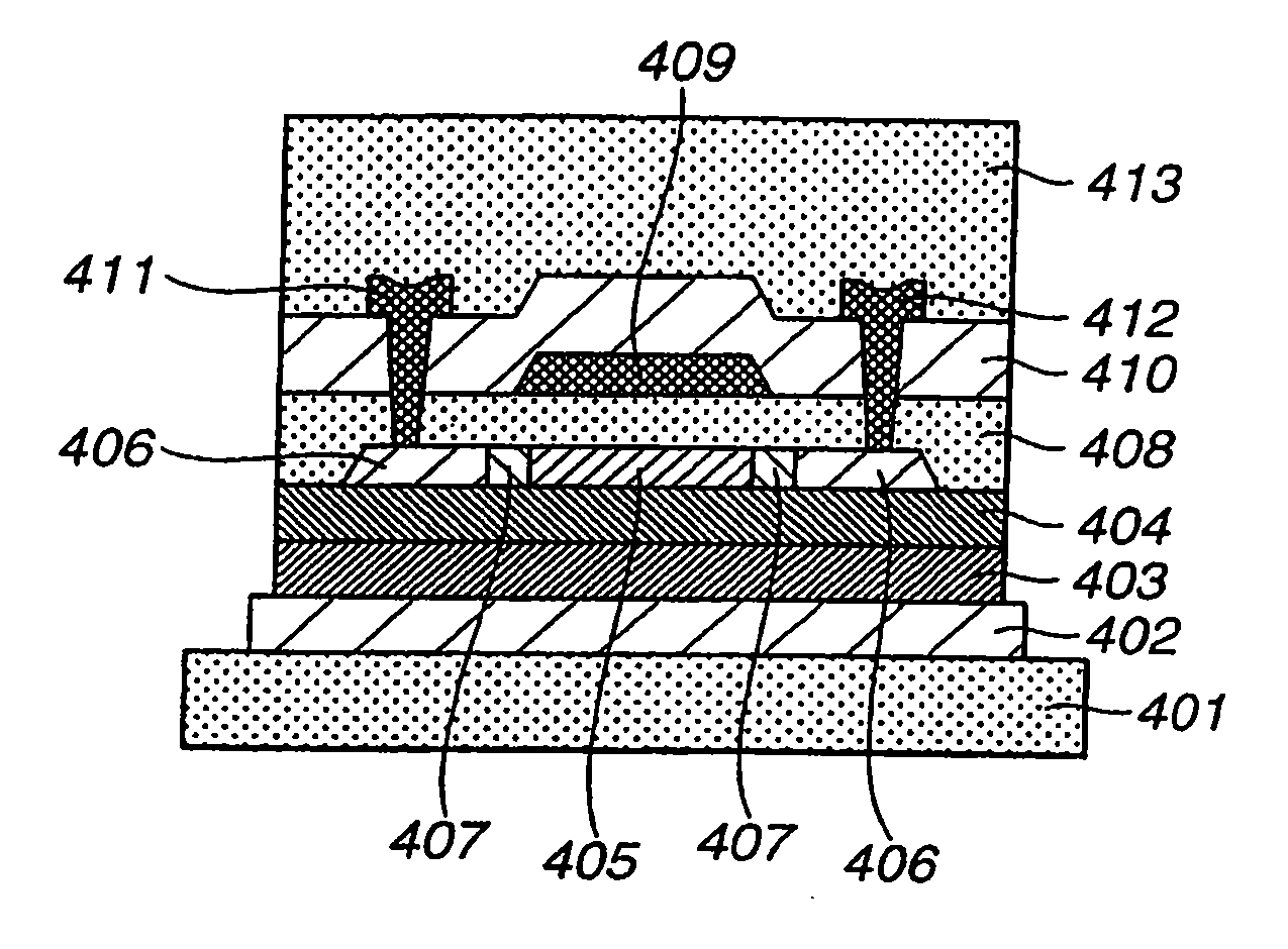
Figure 1 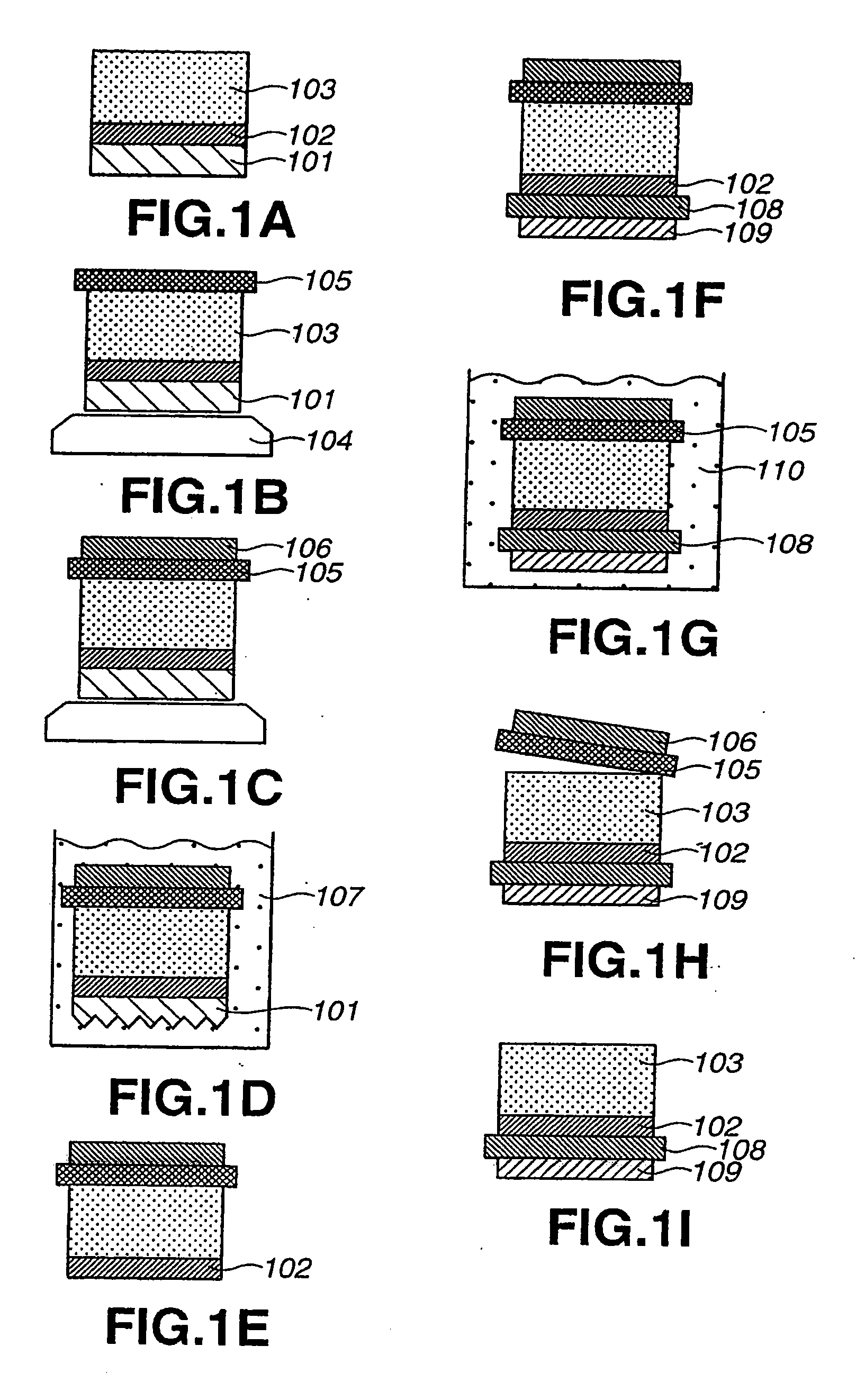
Figure 2 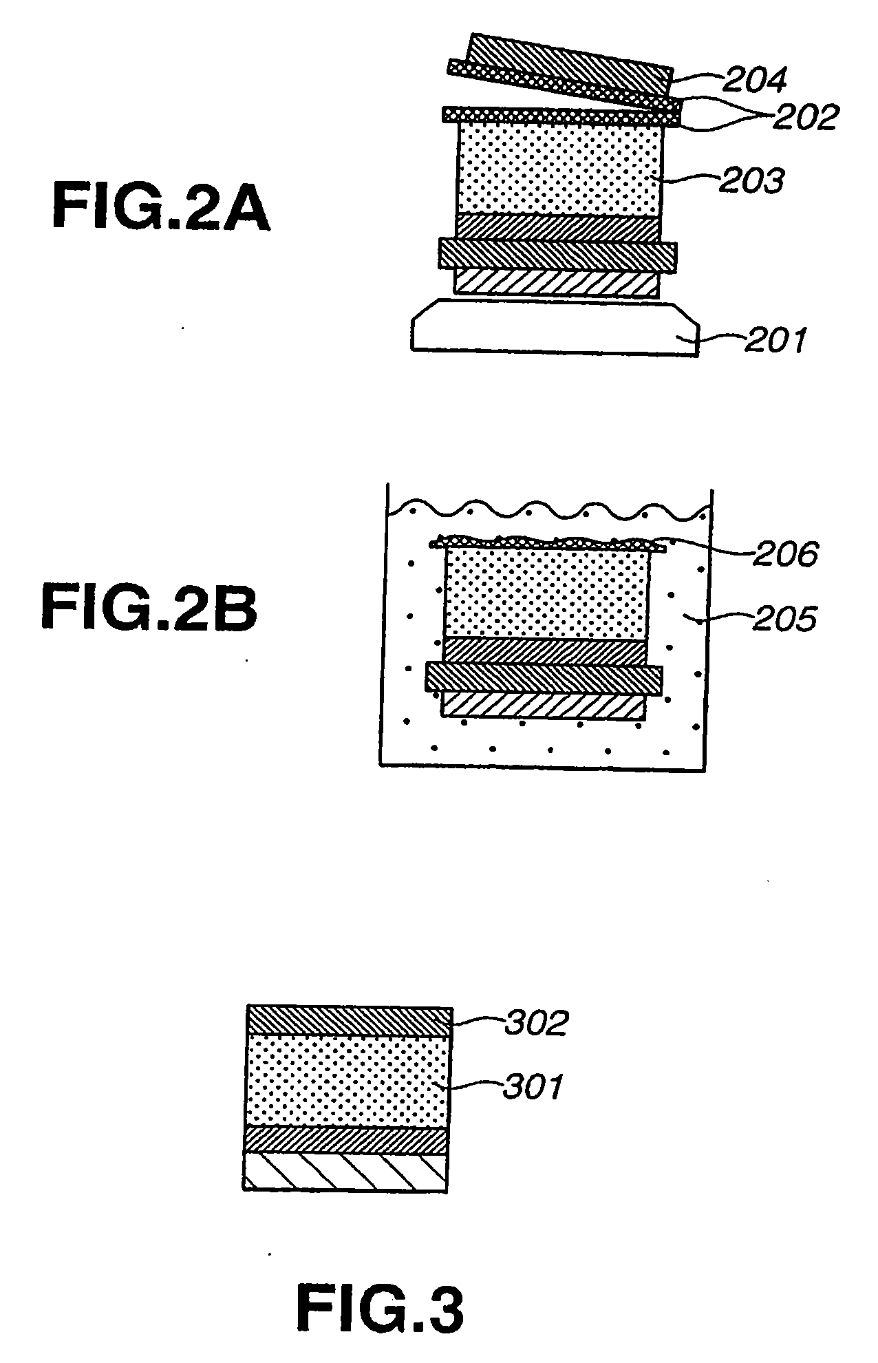
Figure 3
Abstract
Description
CROSS REFERENCE TO RELATED APPLICATIONS
[0001] This is a divisional of co-pending U.S. Ser. No. 11 / 0709,409, filed on Mar. 14, 2005, which is a continuation application of U.S. application Ser. No. 10 / 311,192, filed Dec. 13, 2002, which claims priority based on PCT / JP02 / 03700, filed Apr. 12, 2002, both of which are incorporated herein by reference to the extent permitted by law. This applicant also claims the benefit of priority to Japanese Application No. P2001-115119, filed Apr. 13, 2001.TECHNICAL FIELD
[0002] The present invention relates to a method for manufacturing a thin film device and a semiconductor device, and more particularly, to a method for manufacturing a thin film device used for a flat type display panel employing a liquid crystal or an electroluminescence (abbreviated it as an EL, hereinafter) or the like and forming an active matrix type driving substrate using, for instance, a thin film transistor (Thin Film Transistor, refer it to as a TFT, hereinafter) and a s...
Examples
first embodiment
[0076]FIG. 4 shows a sectional structure of an n channel type top gate TFT on the polyimide substrate manufactured according to the present invention.
[0077] As shown in FIG. 4, on a polyimide substrate 401 having the thickness of 0.25 mm, a molybdenum layer 403 having the thickness of 500 nm and an electrical insulating layer 404 made of an SiO2 layer with the thickness of 500 nm formed by a plasma CVD method or a laminated body of an SiO2 layer and an SiNx layer are formed through an epoxy resin adhesive layer 402. A polysilicon layer 405 serving as a channel forming area is formed thereon and polysilicon layers 406 made of n+ type dope areas and polysilicon layers 407 made of n− type dope areas are formed at both the sides thereof. As described above, an active area has an LDD (Lightly Doped Drain) structure for making a high ON-state current compatible with a low OFF-state current. The polysilicon layers 405, 406 and 407 were manufactured in such a manner that amorphous silicon l...
fourth embodiment
[0088] Now, a fourth embodiment will be described by referring to FIGS. 8A and 8B.
[0089] In the fourth embodiment as shown in FIG. 8A, a molybdenum layer 802, a device layer 803, a hot melt adhesive layer 804 and a molybdenum plate 805 are laminated on a glass substrate 801 and hydrofluoric acid resistant seals 806 are formed on the side surfaces of them.
[0090] The fourth embodiment is different from the first embodiment from the viewpoint that after the molybdenum plate 805 is bonded to the device layer 803, outer peripheral end parts are sealed by the hydrofluoric acid resistant seals 806 made of a resin having a hydrofluoric acid resistance such as a hot melt adhesive as shown in FIG. 8A, before the first substrate (glass substrate) shown in FIG. 1D of the first embodiment is etched. In such a structure, as shown in FIG. 8B, the entry of hydrofluoric acid 807 from end parts during the etching process of the glass substrate 801 could be effectively assuredly prevented by the hydr...
sixth embodiment
[0093] Now, a sixth embodiment will be described by referring to FIGS. 10A to 10E.
[0094] In the sixth embodiment, as shown in FIG. 10A, a laminated body obtained by sequentially laminating a molybdenum thin film 1002, a device layer 1005, a hot melt adhesive 1006, a molybdenum plate 1003 and a polyester film 1004 from a lower layer is immersed in etching solution 1001 for the molybdenum thin film.
[0095] The sixth embodiment is different from the first embodiment in a point of view that after a glass substrate is removed by an etching process by hydrofluoric acid, the laminated body is immersed in the etching solution 1001 composed of mixed acid including phosphoric acid (H3PO4) of 72%, nitric acid (HNO3) of 3%, and acetic acid (CH3COOH) of 10% (the rest is composed of water) to completely remove the molybdenum thin film 1002. Before the etching process, the polyester film 1004 was thermocompression-bonded to the surface of the molybdenum plate 1003 to protect it from the etching pr...