
Delay selecting circuit for semiconductor memory device
a technology of delay selection and memory device, which is applied in the direction of information storage, static storage, digital storage, etc., can solve the problems of increasing the delay amount applied to the command type of signal for securing the appropriate time margin, and the arrival of the command type of signal very la
Patent Information
- Authority / Receiving Office
- US · United States
- Patent Type
- Applications(United States)
- Current Assignee / Owner
- Publication Date
- 2008-04-03
Smart Images
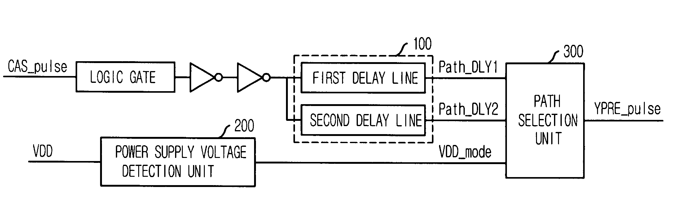
Figure 1 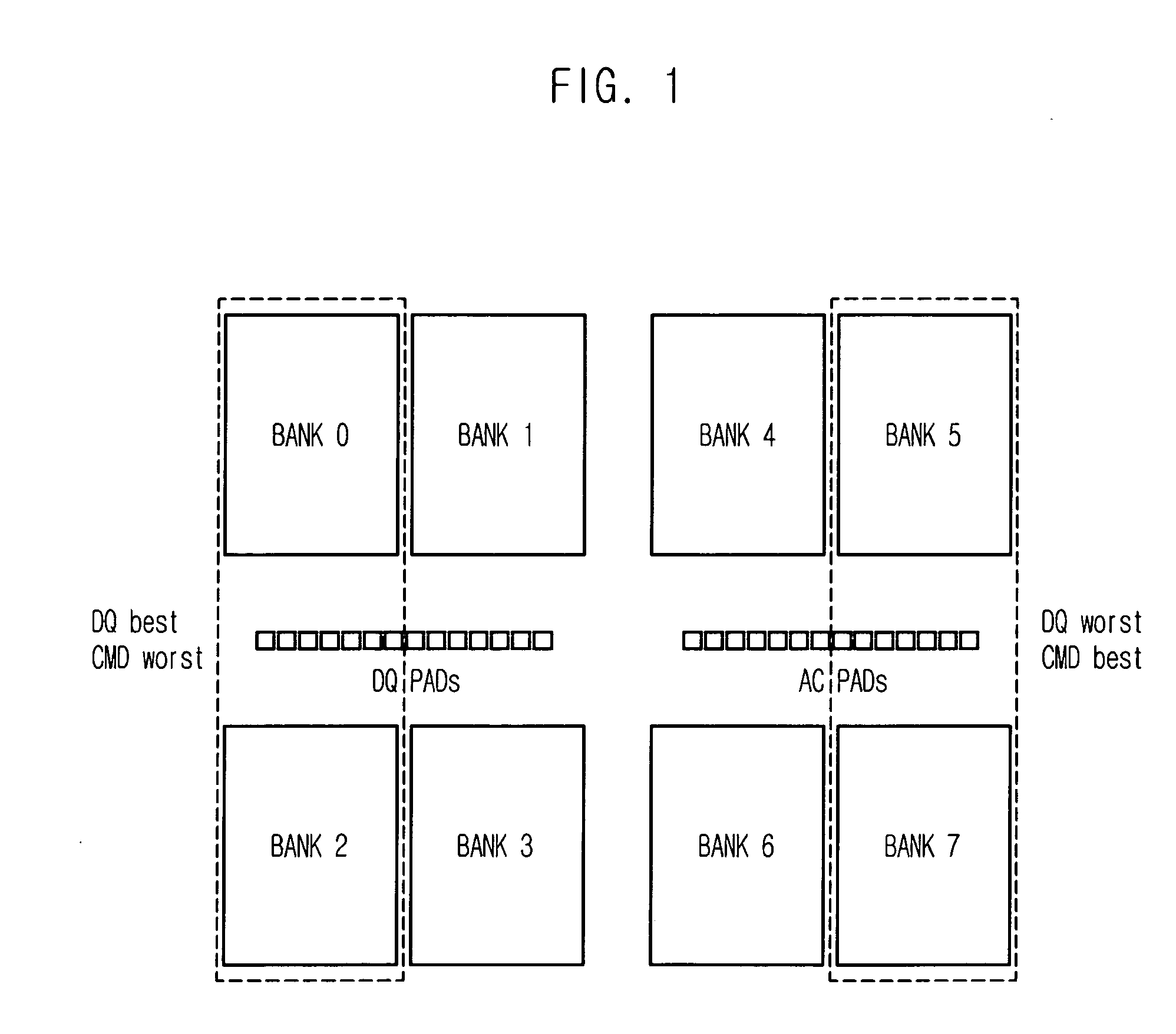
Figure 2 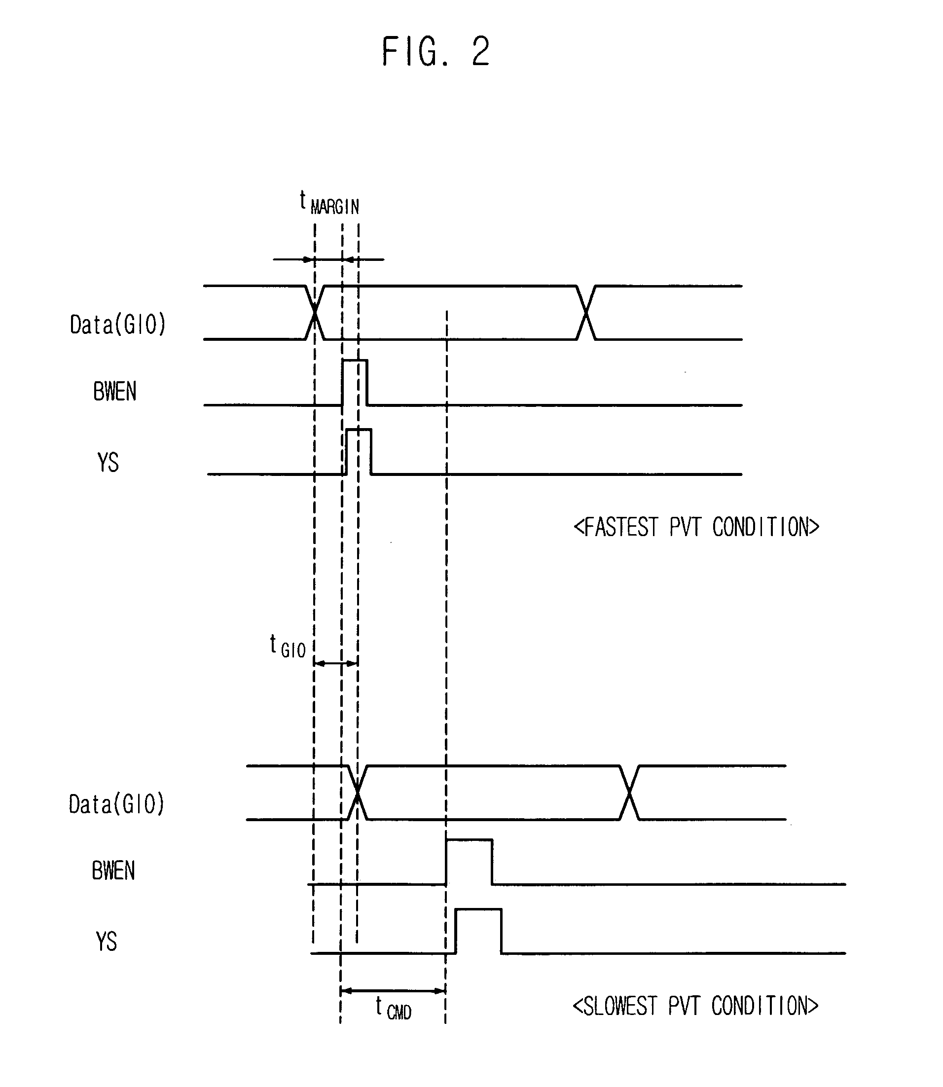
Figure 3
Abstract
Description
CROSS-REFERENCE(S) TO RELATED APPLICATIONS
[0001] The present invention claims priority of Korean patent application no. 10-2006-0096303, filed in the Korean Patent Office on Sep. 29, 2006, which is incorporated by reference in its entirety.BACKGROUND OF THE INVENTION
[0002] The present invention relates to a semiconductor memory device; and, more particularly, to a semiconductor memory device for preventing discordance of a signal timing, which occurs as a chip size and the number of banks are increased in the semiconductor memory device, between data type of signals and command type of signals.
[0003] FIG. 1 illustrates a block diagram showing a semiconductor memory device having eight banks. As capacity of a semiconductor memory device is increased and a semiconductor memory device having high-performance, e.g., a double data rate 3 (DDR3) ram, is developed, a bank structure of the semiconductor memory device has been changed from a conventional 4-bank structure to an 8-bank structure ...
Examples
Embodiment Construction
[0027]Under high level of a power supply voltage, a command type of signal is delayed at a writing operation in order to secure a timing margin. However, a tAA is decreased at a reading operation due to a delayed command type of signal. In accordance with the present invention, it is possible to select a delay amount according to a voltage level of the power supply voltage. Therefore, the above-mentioned problem can be prevented. Further, by adding a storing unit, the problem of a command type of signal having two pulses when the power supply voltage is changed during a short time interval can be solved.
[0028]Hereinafter, a delay selection circuit in accordance with the present invention will be described in detail referring to the accompanying drawings.
[0029]FIG. 3 illustrates a block diagram showing a delay selection circuit for use in a semiconductor memory device in accordance with the present invention. The delay selection circuit includes a delay line unit 100, a power supply ...