
Dislocation reduction in non-polar iii-nitride thin films
a technology of non-polar iii-nitride and thin film, applied in the field of semiconductor materials, can solve problems such as fixed sheet charge formation, and achieve the effect of reducing threading dislocations and reducing threading dislocations
Patent Information
- Authority / Receiving Office
- US · United States
- Patent Type
- Applications(United States)
- Current Assignee / Owner
- Publication Date
- 2008-06-12
- Estimated Expiration
- Not applicable · inactive patent
Smart Images
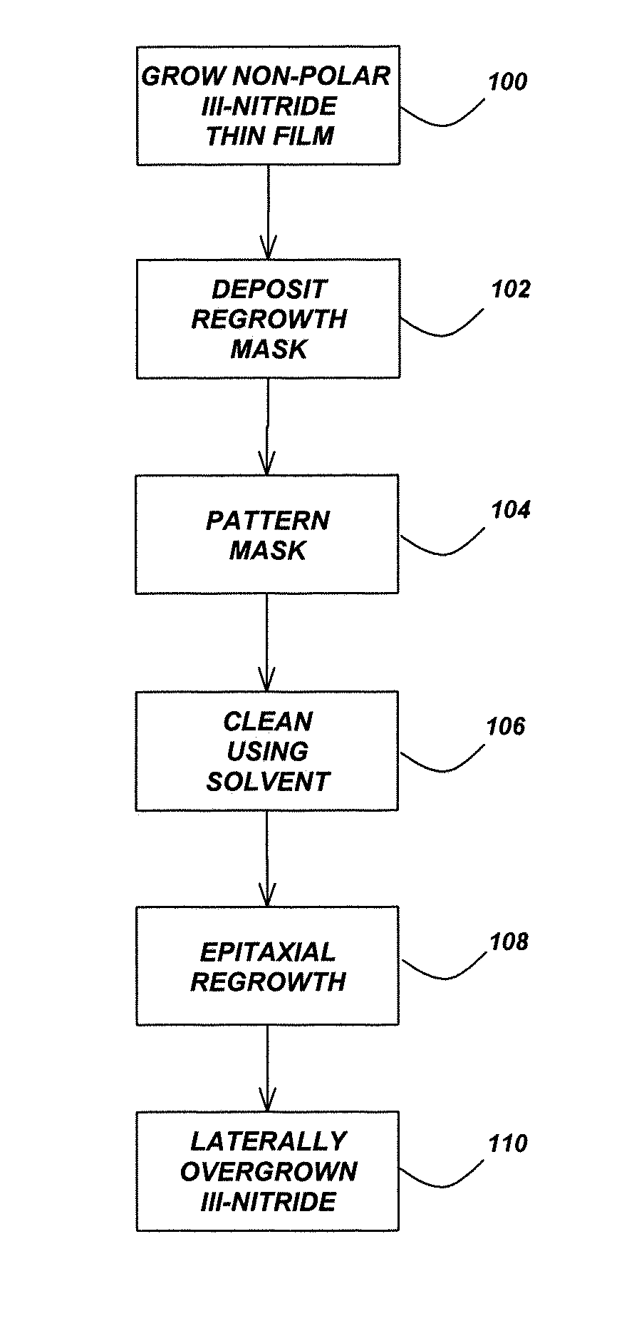
Figure 1 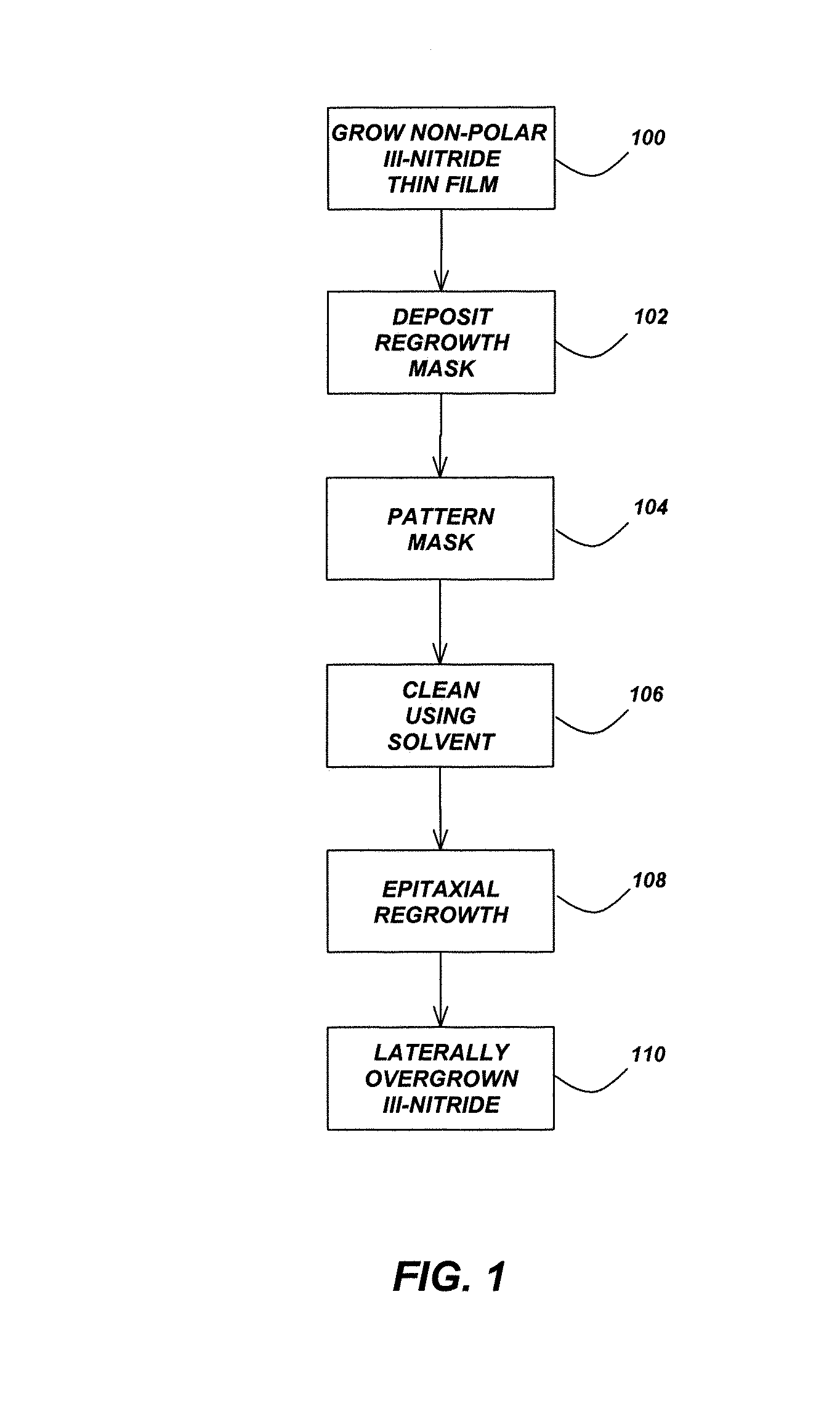
Figure 2 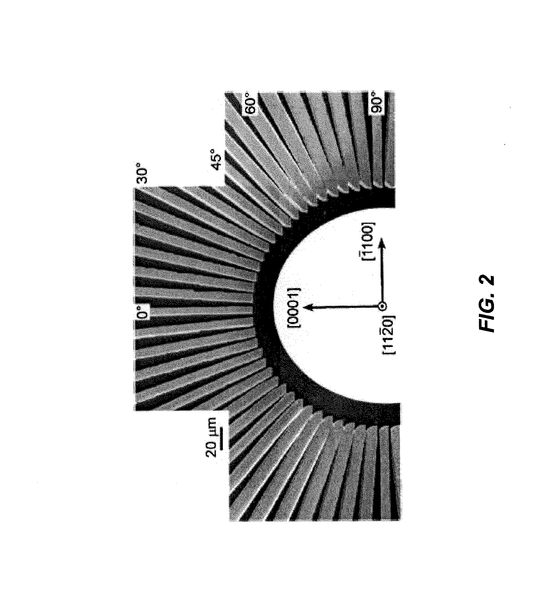
Figure 3
Abstract
Description
CROSS-REFERENCE TO RELATED APPLICATIONS
[0001] This application is a continuation-in-part of the following co-pending applications: U.S. Utility patent application Ser. No. 10 / 413,691, entitled “NON-POLAR A-PLANE GALLIUM NITRIDE THIN FILMS GROWN BY METALORGANIC CHEMICAL VAPOR DEPOSITION,” filed on Apr. 15, 2003, by Michael D. Craven and James S. Speck, attorneys docket number 30794.100-US-U1, which application claims the benefit under 35 U.S.C. § 119(e) of U.S. Provisional Patent Application Ser. No. 60 / 372,909, entitled “NON-POLAR GALLIUM NITRIDE BASED THIN FILMS AND HETEROSTRUCTURE MATERIALS,” filed on Apr. 15, 2002, by Michael D. Craven, Stacia Keller, Steven P. Denbaars, Tal Margalith, James S. Speck, Shuji Nakamura, and Umesh K. Mishra, attorneys docket number 30794.95-US-P1; and
[0002] U.S. Utility patent application Ser. No. 11 / 472,033, entitled “NON-POLAR (Al, B, In, Ga)N QUANTUM WELL AND HETEROSTRUCTURE MATERIALS AND DEVICES,” filed on Jun. 21, 2006, by Michael D. Craven, Staci...
Examples
Embodiment Construction
[0020]In the following description of the preferred embodiment, reference is made to the accompanying drawings which form a part hereof, and in which is shown by way of illustration a specific embodiment in which the invention may be practiced. It is to be understood that other embodiments may be utilized and structural changes may be made without departing from the scope of the present invention.
[0021]Overview
[0022]The present invention reduces threading dislocation densities in non-polar III-nitride through the lateral overgrowth of a planar heteroepitaxial “seed” layer. Lateral overgrowth techniques require a processing step between two MOCVD growths, an initial heteroepitaxial growth and a regrowth that constitutes the lateral overgrowth. First, a thin patterned dielectric mask is applied to the seed layer. Upon regrowth, the III-nitride initially grows vertically through openings in the dielectric mask before laterally overgrowing the mask in directions perpendicular to the ver...