
Switching regulator
Patent Information
- Authority / Receiving Office
- US · United States
- Current Assignee / Owner
- Publication Date
- 2009-12-31
- Estimated Expiration
- Not applicable · inactive patent
Smart Images
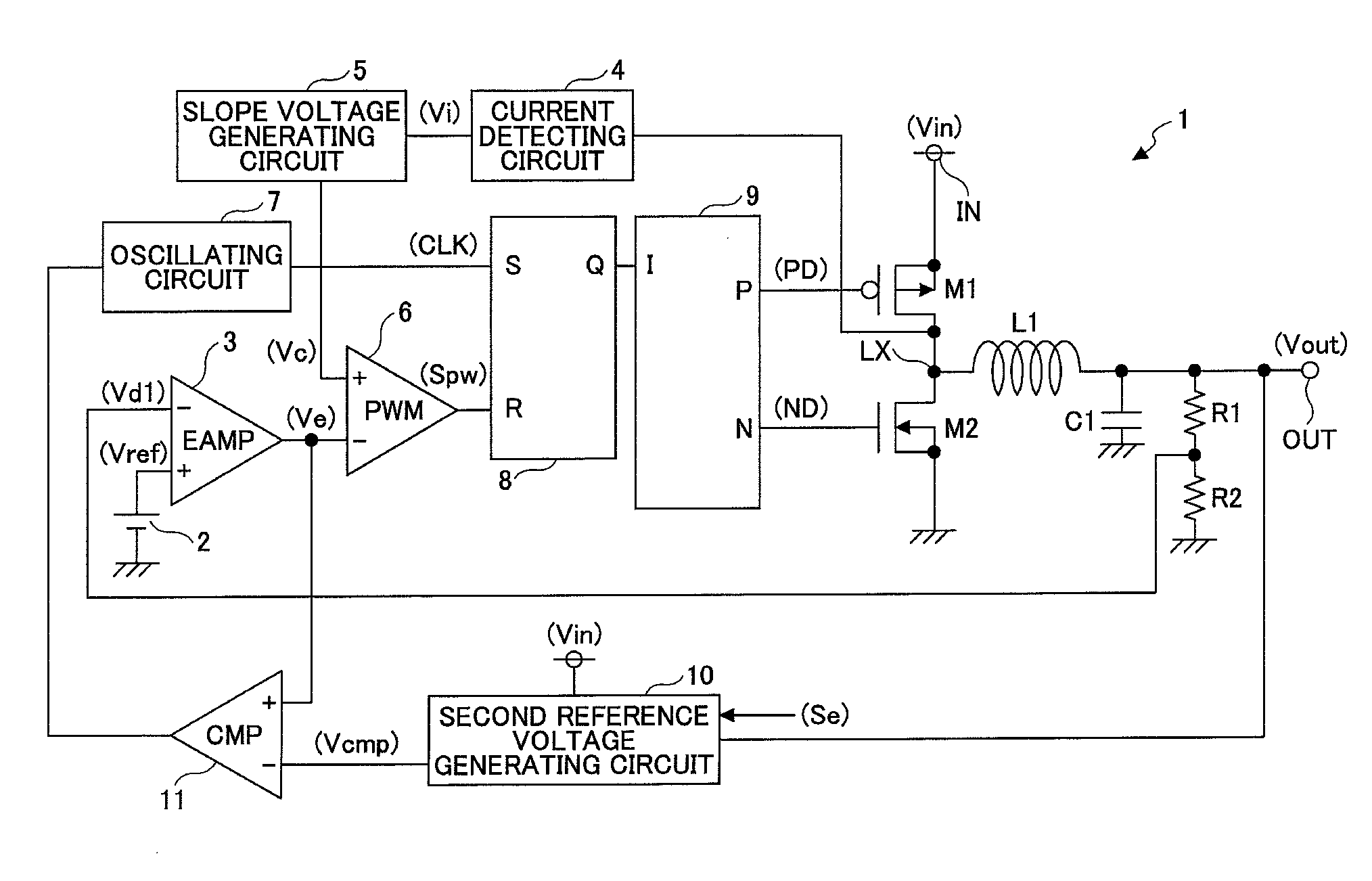
Figure 1 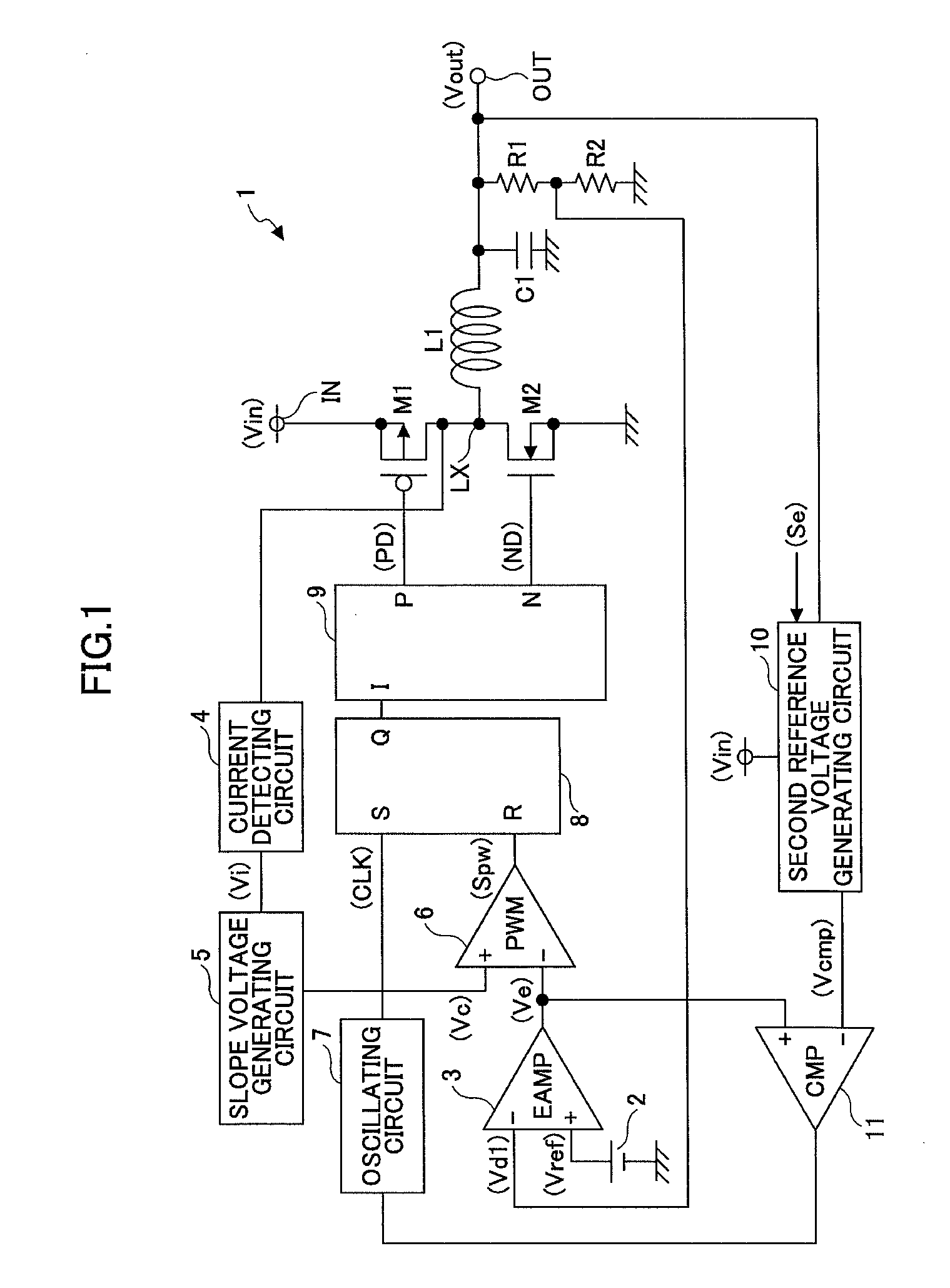
Figure 2 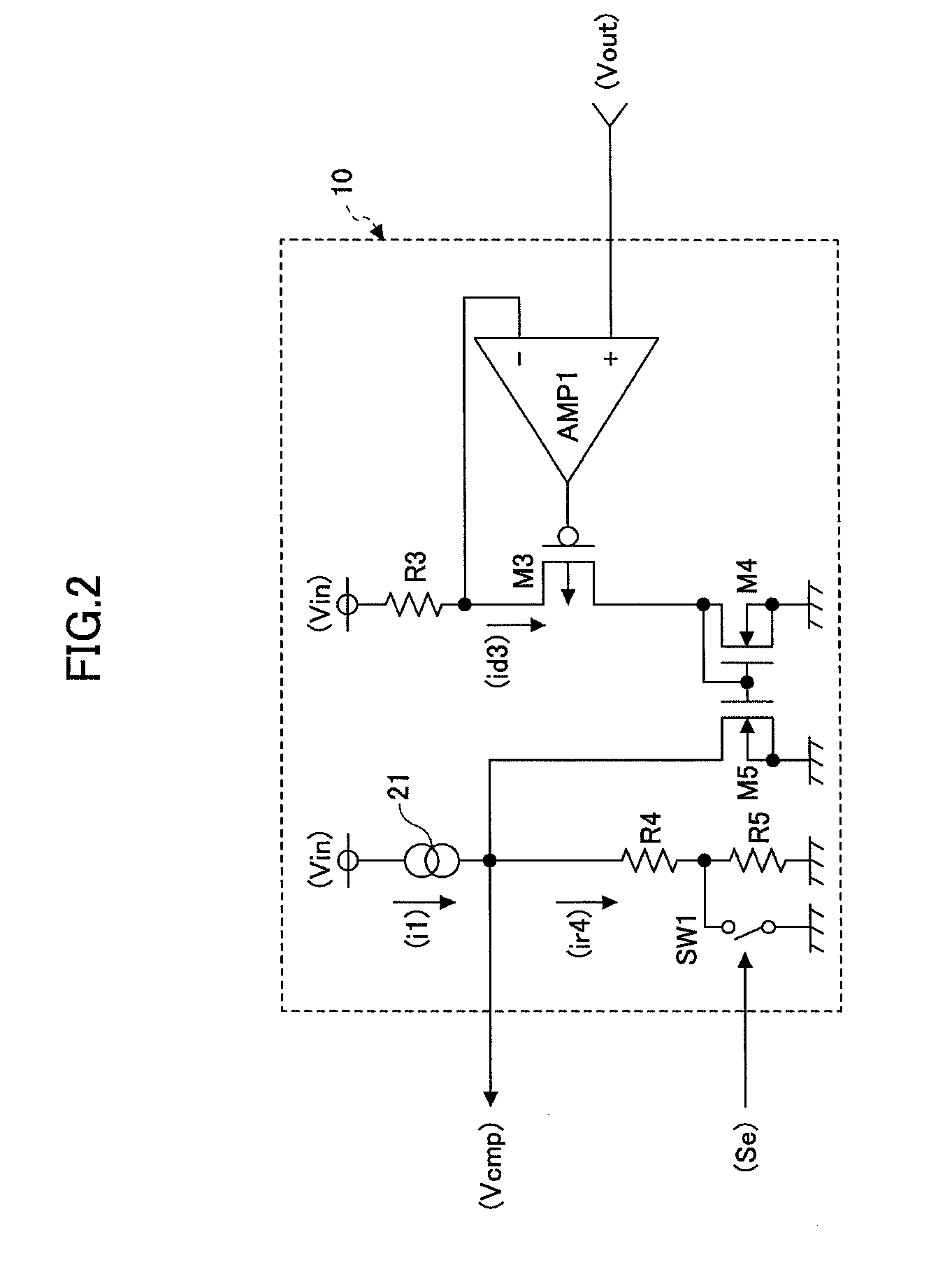
Figure 3
Abstract
Description
BACKGROUND OF THE INVENTION
[0001] 1. Field of the Invention
[0002] The present invention relates to a switching regulator capable of preventing variations in the output voltage and operating by consuming low power, under light load conditions.
[0003] 2. Description of the Related Art
[0004] A conventional switching regulator performs PWM (Pulse Width Modulation) control under regular conditions, and switches to performing VFM (Variable Frequency Modulation) control under light load conditions.
[0005] With PWM control, the constant voltage output operation is performed by fixing the frame frequency and feeding back a monitored output status to adjust the time during which a switch element is turned on in accordance with the fed-back status. Meanwhile, in VFM control, the constant voltage output operation is performed by fixing the time during which the switch element is turned on, or fixing the minimum time during which the switch element is turned on, and feeding back a monitored output stat...
Examples
first embodiment
[0017]FIG. 1 illustrates a circuit example of a switching regulator according to a first embodiment of the present invention.
[0018]A switching regulator 1 constitutes a step-down type switching regulator, in which the current mode can be controlled, for stepping down an input voltage Vin input to an input terminal IN to a predetermined constant voltage, and outputting the voltage as an output voltage Vout from an output terminal OUT.
[0019]The switching regulator 1 includes a switching transistor M1 constituting a PMOS transistor that performs a switching operation for controlling the output of the input voltage Vin; a synchronous rectification transistor M2 constituting an NMOS transistor; an inductor L1; an output capacitor C1; and resistors R1 and R2 used for detecting the output voltage, and generating and outputting a division voltage Vd1 obtained by dividing the output voltage Vout. Furthermore, the switching regulator 1 includes a first reference voltage generating circuit 2 f...