
Nitride semiconductor, nitride semiconductor crystal growth method, and nitride semiconductor light emitting element
a nitride semiconductor and crystal growth technology, applied in the direction of crystal growth process, polycrystalline material growth, chemically reactive gas, etc., can solve the problem of high dislocation density, insufficient dislocation density of ingan in blue-color light-emitting regions normally used as quantum well layers of gan-based leds, and unavoidable gan crystal epitaxial growth on sapphire substrates. , to achieve the effect of improving the crystallinity of the n
Patent Information
- Authority / Receiving Office
- US · United States
- Patent Type
- Applications(United States)
- Current Assignee / Owner
- Publication Date
- 2010-09-30
Smart Images
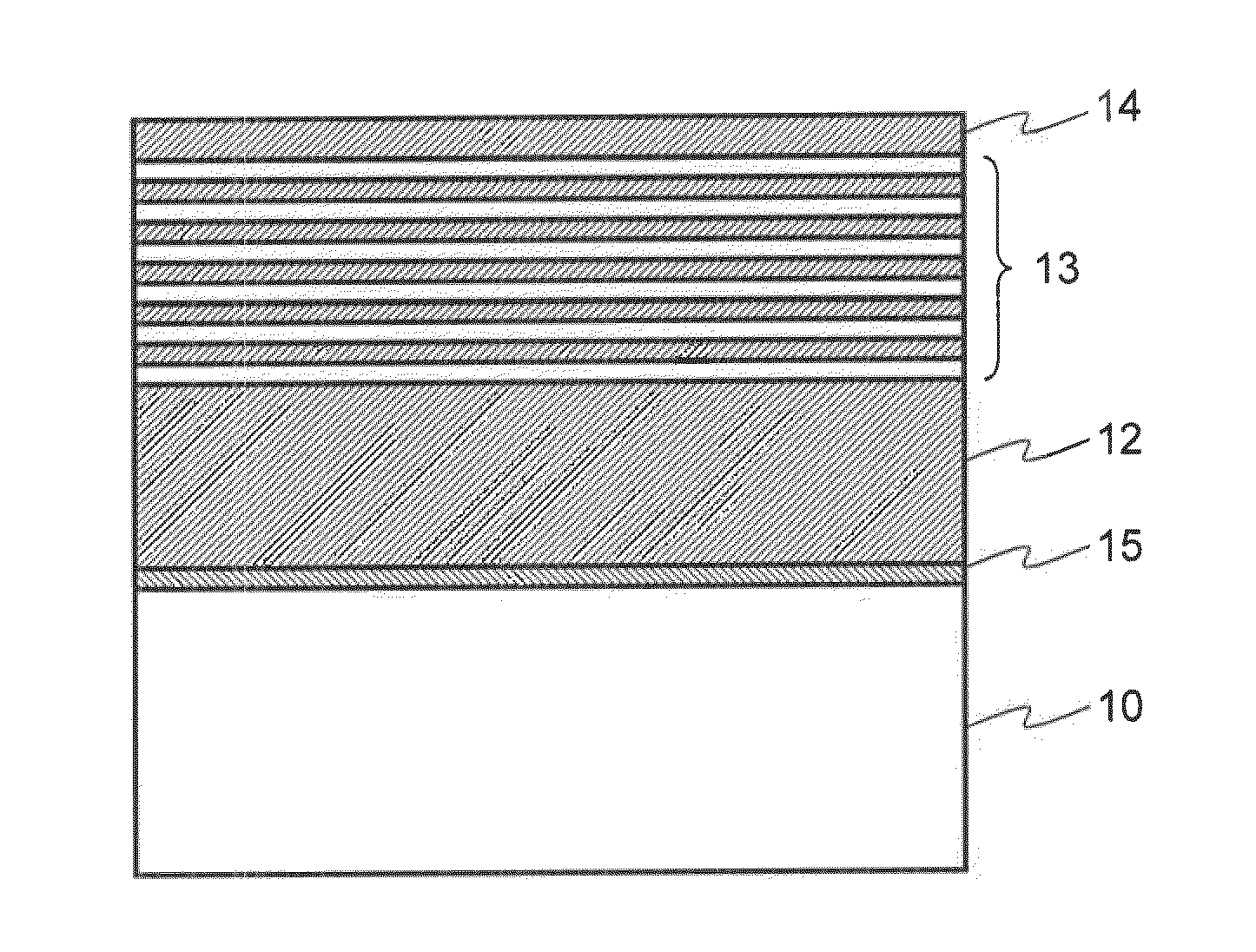
Figure 1 
Figure 2 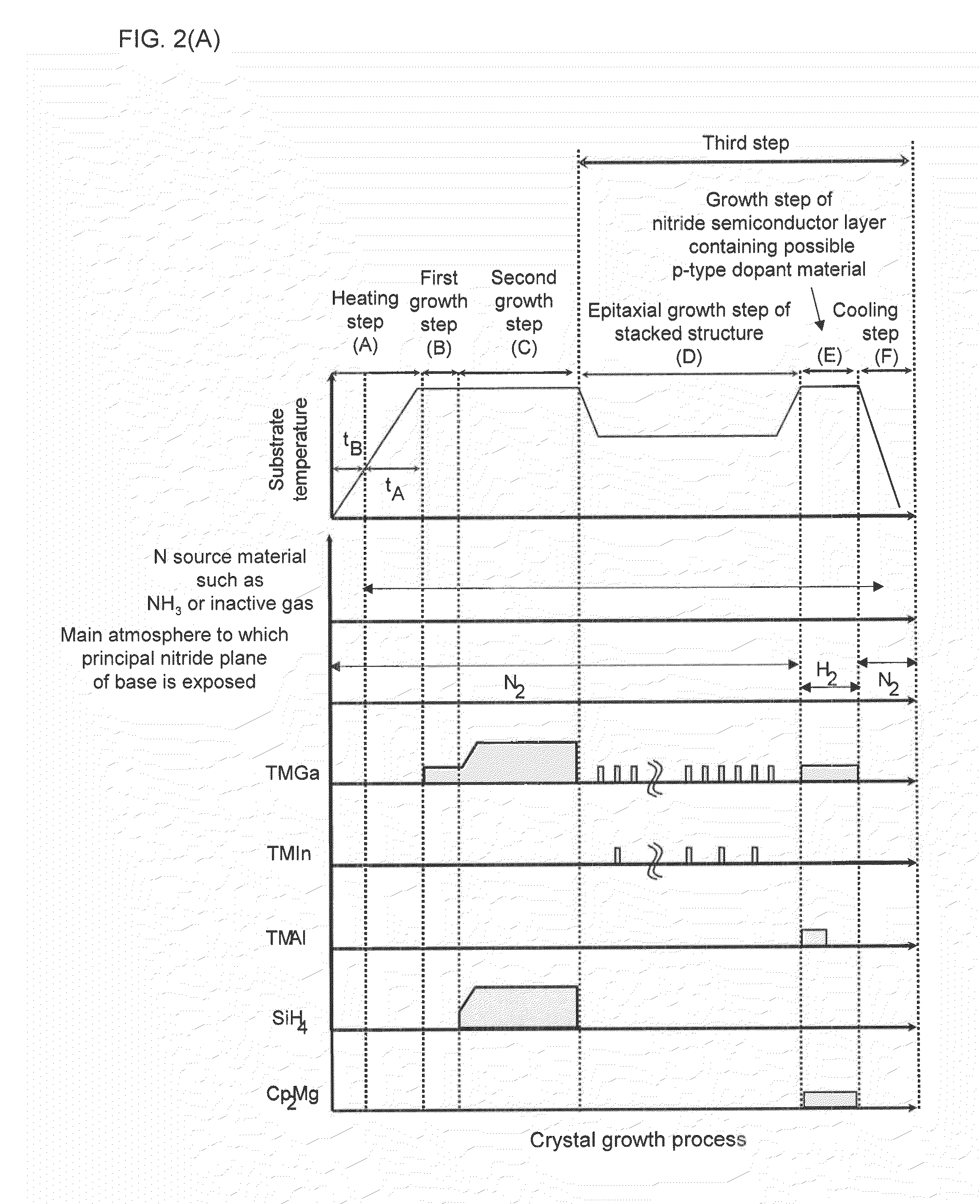
Figure 3
Abstract
Description
TECHNICAL FIELD
[0001] The present invention relates to a nitride semiconductor crystal growth technique, and more particularly, to a crystal growth technique for obtaining a high-quality nitride semiconductor with excellent surface conditions and optical characteristics.BACKGROUND ART
[0002] A blue-color light-emitting element or ultraviolet light-emitting element can be used as a white light source if combined with an appropriate wavelength conversion material. Active studies have been conducted on applications of such white light sources to backlights for liquid crystal displays and the like, light-emitting diode illumination, automotive lighting, general lighting to replace fluorescent lighting, and so on. Some of the studies have already been put to practical use. Today, such blue-color light-emitting elements and ultraviolet light-emitting elements are produced mainly by growing a thin film of gallium nitride-based semiconductor crystal using a technique such as a metal-organic ...
Examples
example 1
[0226]In the present example, a stack of gallium nitride-based semiconductor thin films was grown by the MOCVD process and a near ultraviolet LED was fabricated. A series of crystal growth processes for that has already been outlined with reference to FIG. 2(A). Also, a layer structure after growth is schematically shown in FIG. 3(A).
[0227]The base used was a (1-100) m-plane oriented freestanding GaN substrate. The substrate measured 4.1 mm in the c-axis direction and 15 mm in the a-axis direction. Regarding electrical characteristics, the substrate was n-type and carrier density was 6.6×1017 cm−3. As a result of X-ray diffraction, the full-width at half maximum of a (10-12) reflection rocking curve was 34.2 arcsec., OFF angle in the c(+) direction was 0.25 degrees, and OFF angle in the A direction was 0.03 degrees. Also, the dislocation density was 5.0×106 cm−2.
[0228]The m-plane freestanding GaN substrate was placed on a tray (susceptor) in a horizontal quartz reactor which normall...
example 2
[0244]In the present example, a stack of gallium nitride-based semiconductor thin films was grown by the MOCVD process and a near ultraviolet LED was fabricated. A series of crystal growth processes for that has already been outlined with reference to FIG. 2(A). Also, a layer structure after growth is schematically shown in FIG. 3(A).
[0245]The base used was a (1-100) m-plane oriented freestanding GaN substrate. The substrate measured 4.2 mm in the c-axis direction and 15 mm in the a-axis direction. Regarding electrical characteristics, the substrate was n-type and carrier density was 6.7×1017 cm−3. As a result of X-ray diffraction, the full-width at half maximum of a (10-12) reflection rocking curve was 32.8 arcsec., OFF angle in the c(+) direction was 0.29 degrees, and OFF angle in the a direction was 0.05 degrees. Also, the dislocation density was 5.4×106 cm−2. The m-plane freestanding GaN substrate was placed on a tray (susceptor) in a horizontal quartz reactor which normally ope...
example 3
[0253]In the present example, a stack of gallium nitride-based semiconductor thin films was grown by the MOCVD process and a near ultraviolet LED was fabricated. A series of crystal growth processes for that has already been outlined with reference to FIG. 2(A). Also, a layer structure after growth is schematically shown in FIG. 3(A).
[0254]The base used was a (1-100) m-plane oriented freestanding GaN substrate. The substrate measured 4.0 mm in the c-axis direction and 15 mm in the a-axis direction. Regarding electrical characteristics, the substrate was n-type and carrier density was 6.4×1017 cm−3. As a result of X-ray diffraction, the full-width at half maximum of a (10-12) reflection rocking curve was 36.7 arcsec., OFF angle in the c(+) direction was 3.0 degrees, and OFF angle in the a direction was 0.3 degrees. Also, the dislocation density was 5.1×106 cm−2. The m-plane freestanding GaN substrate was placed on a tray (susceptor) in a horizontal quartz reactor which normally opera...