
Methods of forming conductive layer patterns using gas phase cleaning process and methods of manufacturing semiconductor devices
Patent Information
- Authority / Receiving Office
- US · United States
- Current Assignee / Owner
- Publication Date
- 2011-11-17
Smart Images
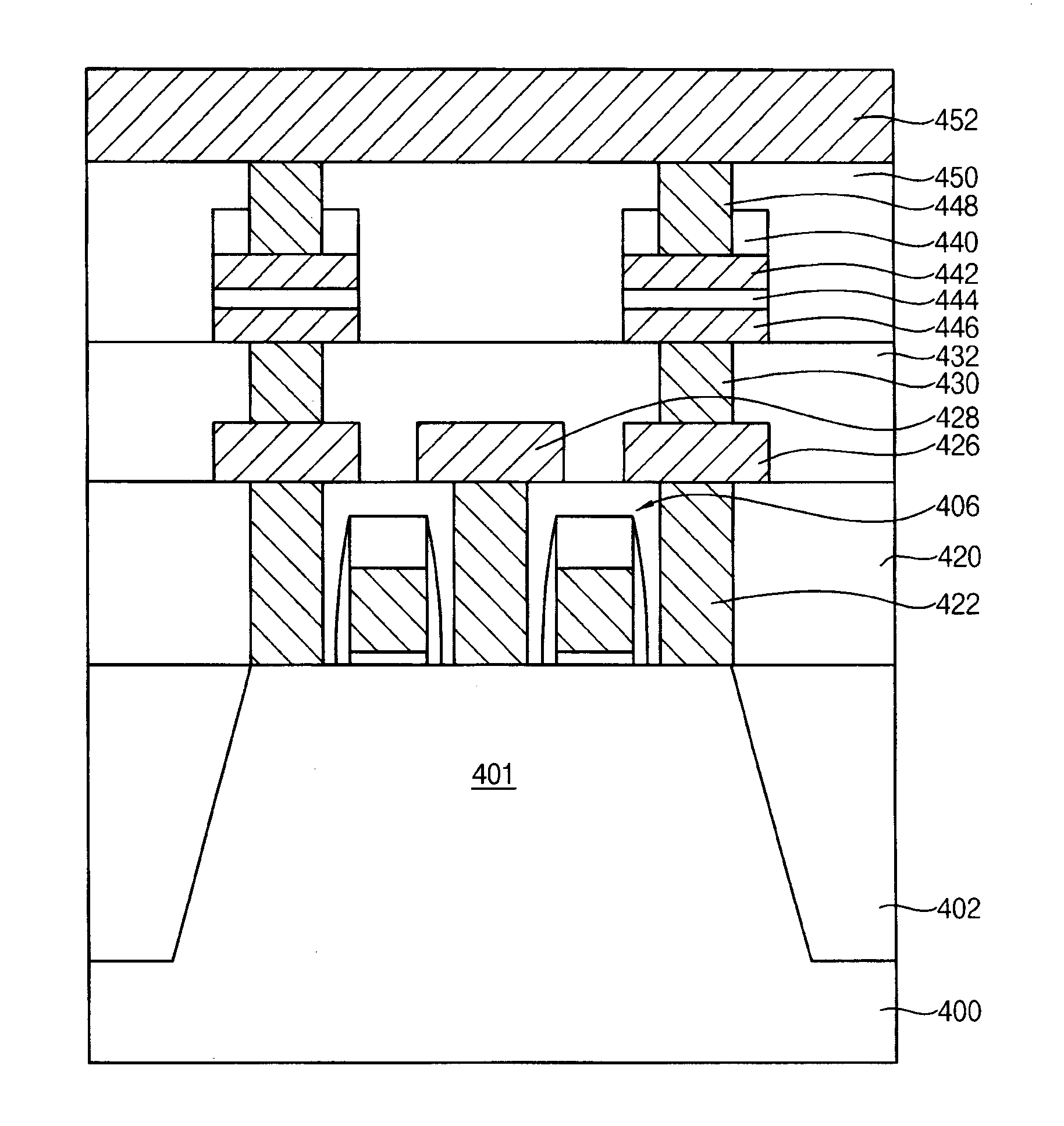
Figure 1 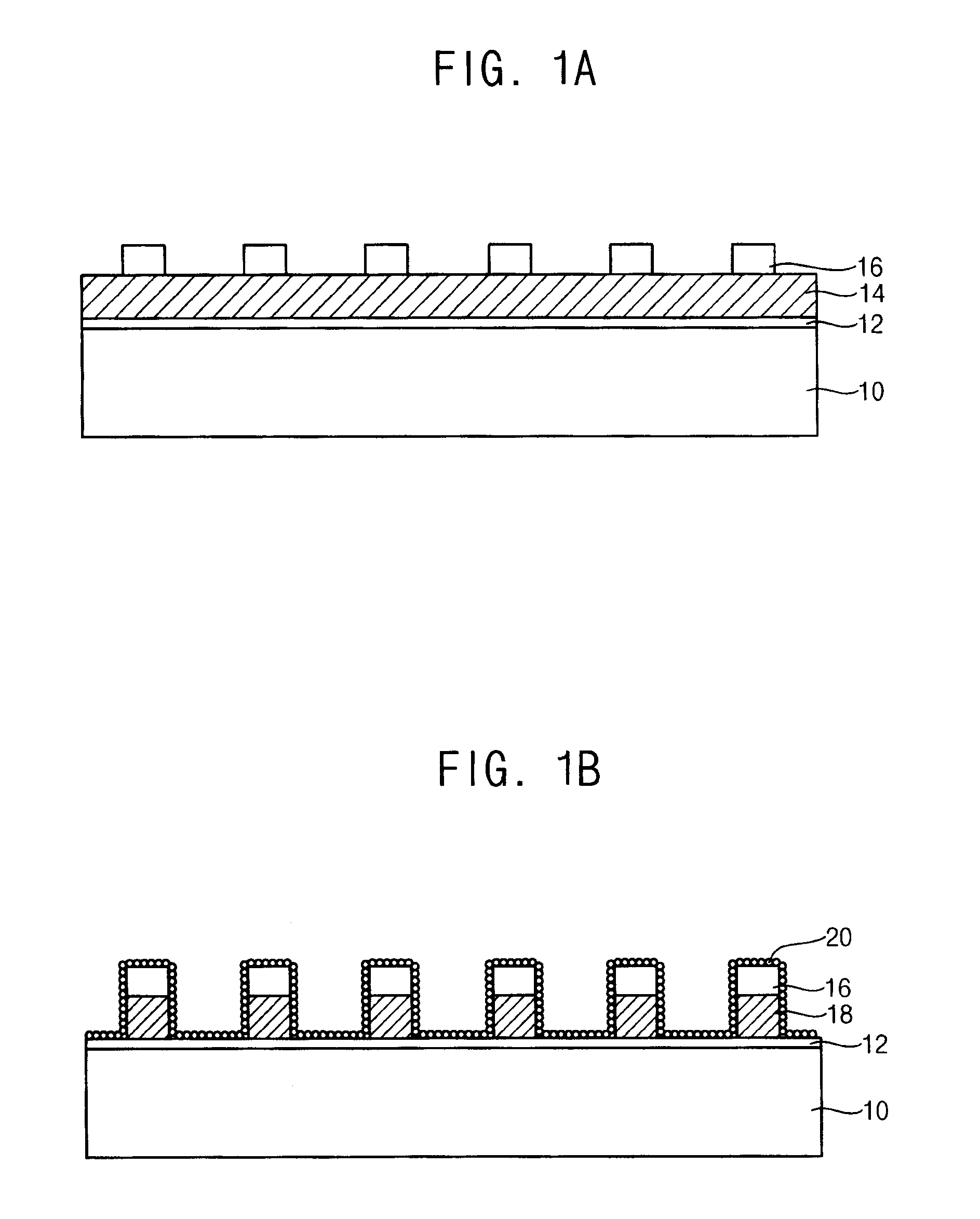
Figure 2 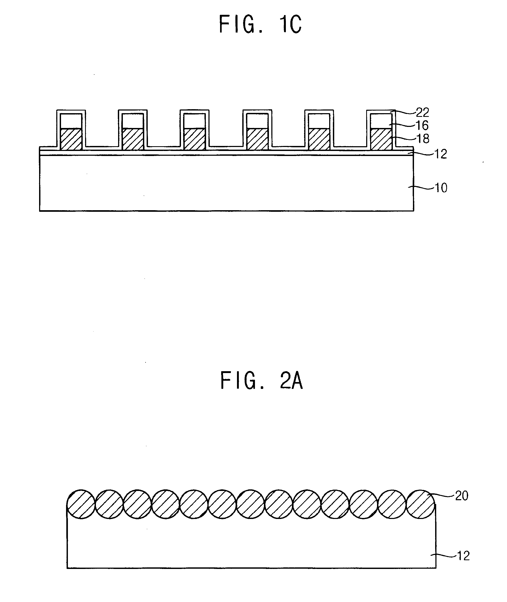
Figure 3
Abstract
Description
CROSS-REFERENCE TO RELATED APPLICATIONS
[0001] This application claims priority under 35 USC §119 from Korean Patent Application No. 10-2010-0043835, filed on May 11, 2010 in the Korean Intellectual Property Office (KIPO), the disclosure of which is incorporated herein by reference in its entirety.BACKGROUND
[0002] 1. Field of the General Inventive Concept
[0003] The general inventive concept relates to methods of forming a conductive layer pattern using a gas phase cleaning process and methods of manufacturing a semiconductor device using the methods of forming the conductive layer pattern.
[0004] 2. Description of the Related Art
[0005] As semiconductor devices have been highly integrated, physical sizes of various structures constituting the semiconductor devices including a line width and spaces of cell transistors and metal wirings, a size of capacitors, etc., have become remarkably decreased. Recently, dynamic random access memory (DRAM) devices having a critical size of about 40 nm hav...
Examples
Embodiment Construction
[0085]Various example embodiments will be described more fully hereinafter with reference to the accompanying drawings, in which some example embodiments are illustrated. Reference will now be made in detail to the embodiments of the present general inventive concept, examples of which are illustrated in the accompanying drawings, wherein like reference numerals refer to the like elements throughout. The embodiments are described below in order to explain the present general inventive concept while referring to the figures. The present general inventive concept may, however, be embodied in many different forms and should not be construed as limited to the example embodiments set forth herein. Rather, these example embodiments are provided so that this description will be thorough and complete, and will convey the scope of the present general inventive concept to those skilled in the art. In the drawings, the sizes and relative sizes of layers and regions may be exaggerated for clari...