
Electrostatic Discharge Protection Device Comprising a Silicon Controlled Rectifier
a technology of electronic discharge protection and rectifier, which is applied in the direction of semiconductor devices, semiconductor/solid-state device details, diodes, etc., can solve the problems of latching during testing or thereafter, early trigger of mos devices is unwanted, and trigger voltage too high to be usable in many designs, etc., to achieve higher resistivity, reduce trigger voltage, and reduce the effect of trigger voltag
Patent Information
- Authority / Receiving Office
- US · United States
- Patent Type
- Applications(United States)
- Current Assignee / Owner
- Publication Date
- 2017-01-12
Smart Images
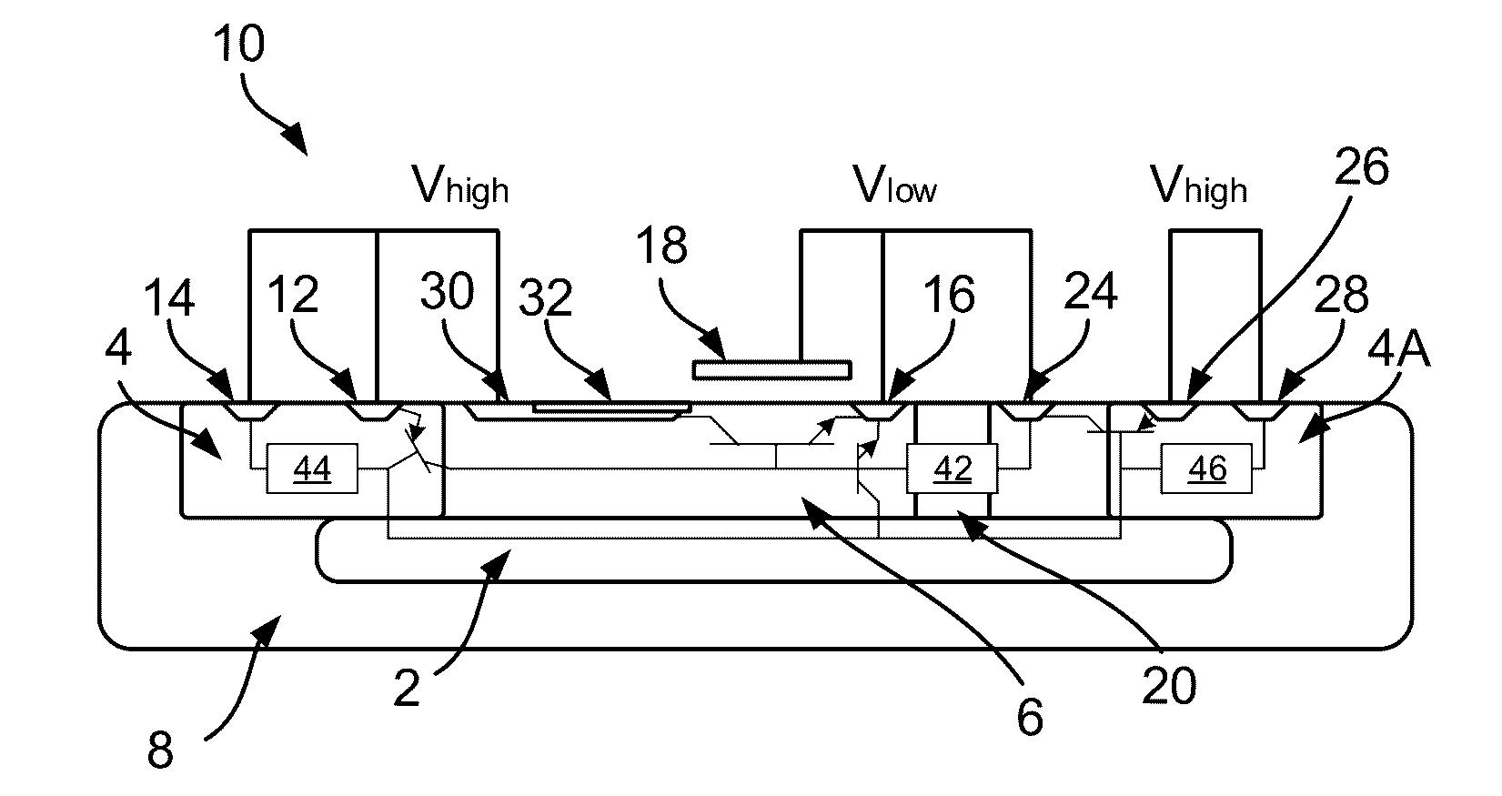
Figure 1 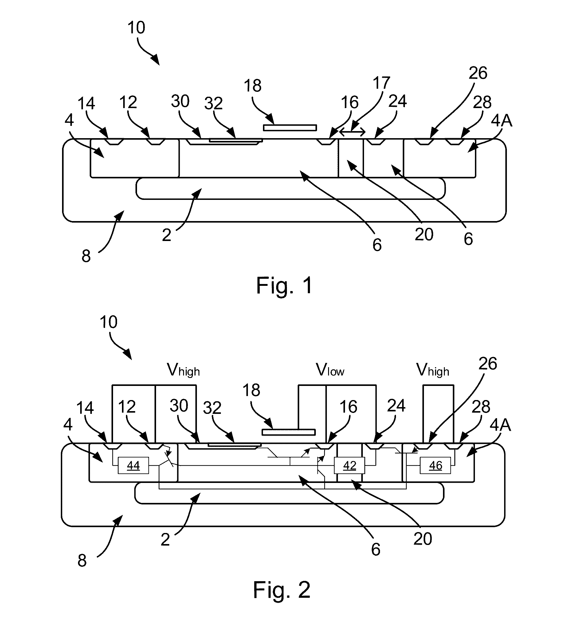
Figure 2 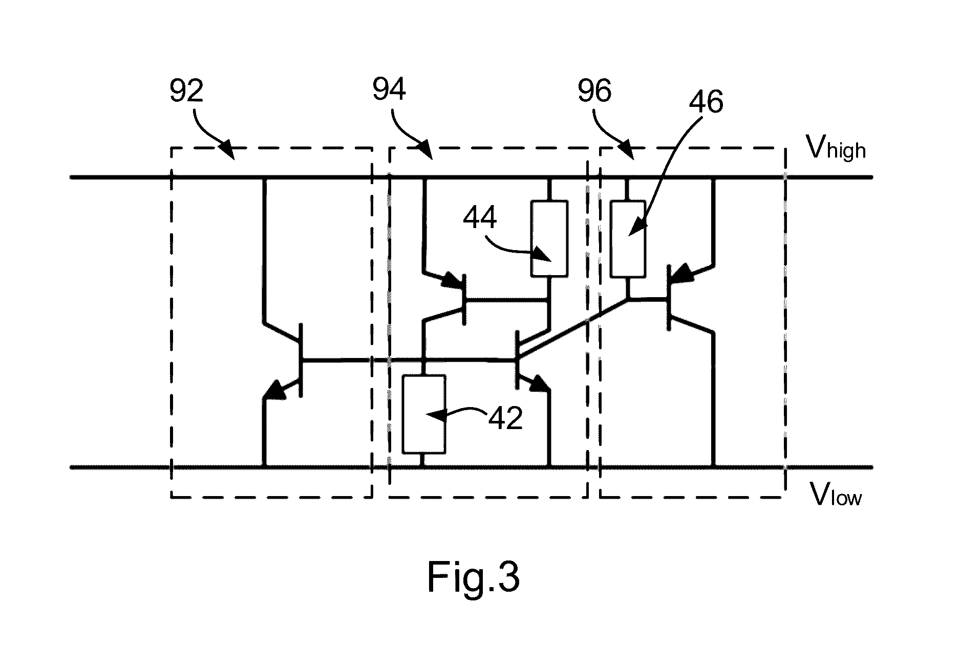
Figure 3
Abstract
Description
FIELD OF THE INVENTION
[0001] This invention relates to an electrostatic discharge protection device comprising a silicon controlled rectifier.BACKGROUND OF THE INVENTION
[0002] Integrated circuits generally include an electrostatic discharge (ESD) device for shunting currents which occur during the manufacturing process (e.g. due to discharging of a charged human body (‘human body model’, or ‘HBM’)). In pad-based ESD designs, in particular, the ESD protection is usually placed locally, and is connected to the drains of an output stage MOS. During an ESD event, current shunting occurs after a trigger voltage across the ESD device has been reached. When the ESD device triggers, its voltage drops to a holding voltage. The trigger voltage of the ESD device should therefore be above a maximum operating voltage of the product.
[0003] A challenge related to pad-based ESD design is that the ESD protection device often has a higher trigger voltage than the trigger voltage of a driver MOS device t...
Examples
Embodiment Construction
[0043]Embodiments of the present disclosure are described in the following with reference to the accompanying drawings.
[0044]Embodiments of this disclosure may provide an electrostatic discharge (ESD) protection device that comprises a silicon controlled rectifier (SCR). The device can be provided in a semiconductor substrate, such as a silicon substrate.
[0045]The following embodiments are described in the context of devices for which the first conductivity type is n-type and the second conductivity type is p-type. Nevertheless, as noted above, it is envisaged that the first conductivity type may be p-type and the second conductivity type may be n-type.
[0046]The device includes region having a first conductivity type (in the examples described below, a first n-type region) located in the substrate. The device includes region having a second conductivity type (in the examples described below, a first p-type region), which is also located in the substrate. The region having the second...