
Complementary-type SCR (Silicon Controlled Rectifier) structure triggered by diode string in an auxiliary way
A diode string and complementary technology, applied in the direction of electrical components, electric solid devices, circuits, etc., can solve the problems of high trigger voltage avalanche breakdown voltage, difficulty in applying integrated circuit ESD protection, etc., and achieve small silicon chip area and low trigger The effect of voltage
Patent Information
- Authority / Receiving Office
- CN · China
- Current Assignee / Owner
- Publication Date
- 2010-07-07
- Estimated Expiration
- Not applicable · inactive patent
Smart Images
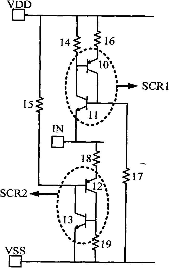
Figure 1 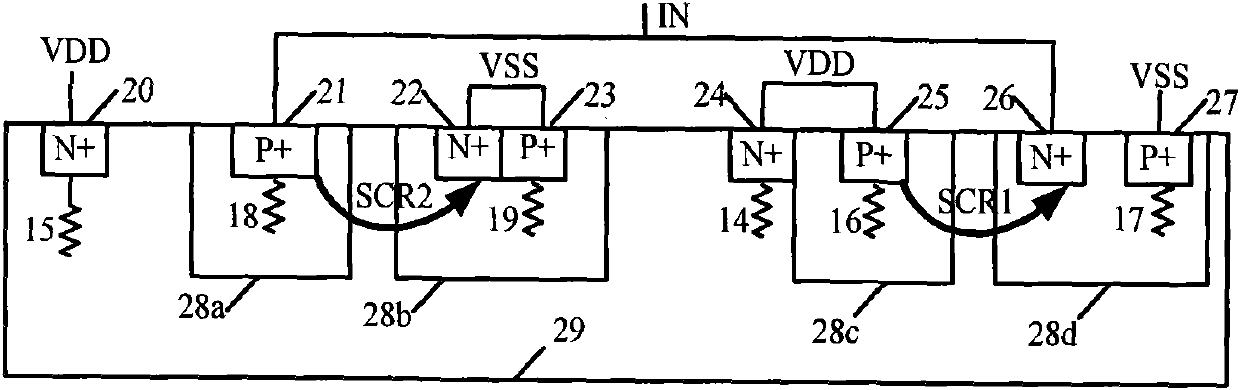
Figure 2 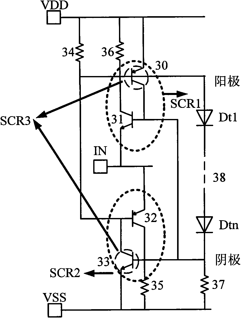
Figure 3
Abstract
Description
technical field
[0001] The invention belongs to the field of integrated circuits, in particular to a complementary SCR structure used to improve the reliability of integrated circuit ESD protection. Background technique
[0002] The phenomenon of electrostatic discharge (ESD) in nature is the most important reliability problem that causes the failure of integrated circuit products. Relevant research surveys show that 30% of integrated circuit failure products are caused by electrostatic discharge phenomena. Therefore, improving the reliability of integrated circuit electrostatic discharge protection has a non-negligible effect on improving the yield of products and even driving the entire national economy.
[0003] Electrostatic discharge phenomenon is usually divided into three discharge modes according to the source of charge: HBM (Human Body Discharge Model), MM (Machine Discharge Mode), and CDM (Component Charge Discharge Mode). The two most common electrostatic discha...
Examples
Embodiment Construction
[0054] A kind of complementary SCR structure of diode string auxiliary triggering of the present invention, its equivalent circuit diagram is as follows image 3 As shown, it includes:
[0055] The first thyristor SCR1 is composed of a first bipolar transistor 30 and a second bipolar transistor 31, wherein the emitter of the first bipolar transistor 30 is connected to the positive power supply line VDD, and the emitter of the first bipolar transistor 30 The base is connected to the positive power supply line VDD through the N-well resistor 36; the emitter of the second bipolar transistor 31 is connected to the chip pin IN to be protected, and the base of the second bipolar transistor 31 is connected to the VDD through the P-well resistor 37. Negative power supply line VSS;
[0056] The second thyristor SCR2 is composed of a third bipolar transistor 32 and a fourth bipolar transistor 33, wherein the emitter of the third bipolar transistor 32 is connected to the chip pin IN to ...