

Standard cell architecture with at least one gate contact over an active area
Patent Information
- Authority / Receiving Office
- US · United States
- Current Assignee / Owner
- Publication Date
- 2018-07-26
Smart Images
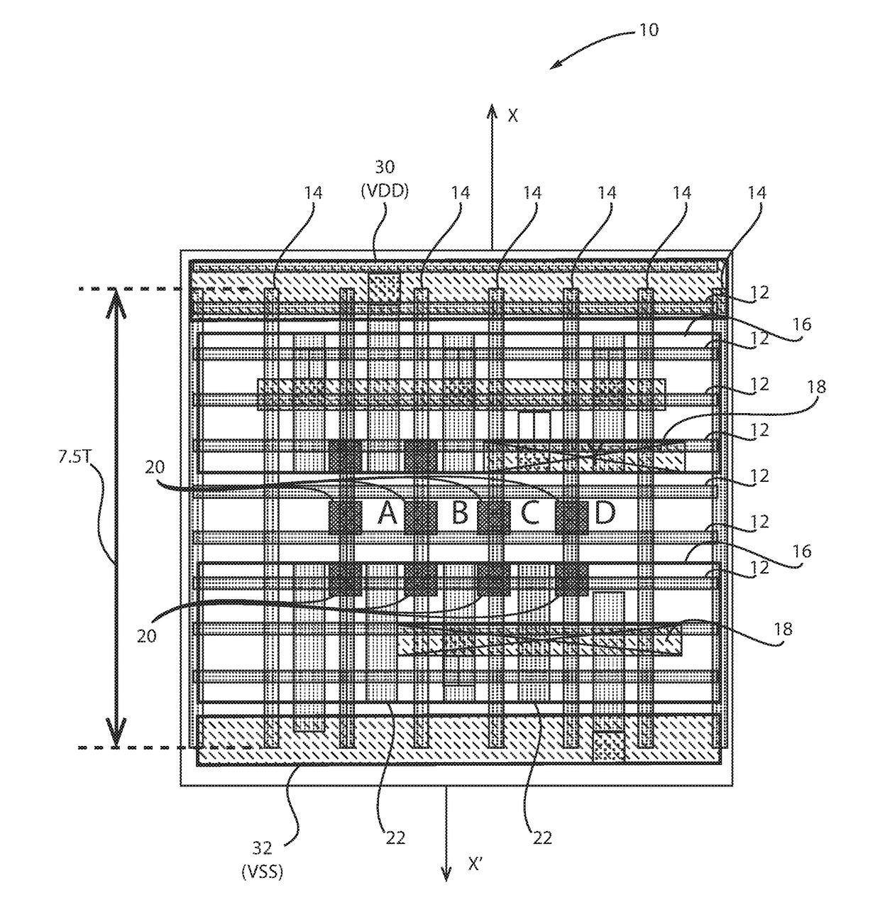
Figure 1 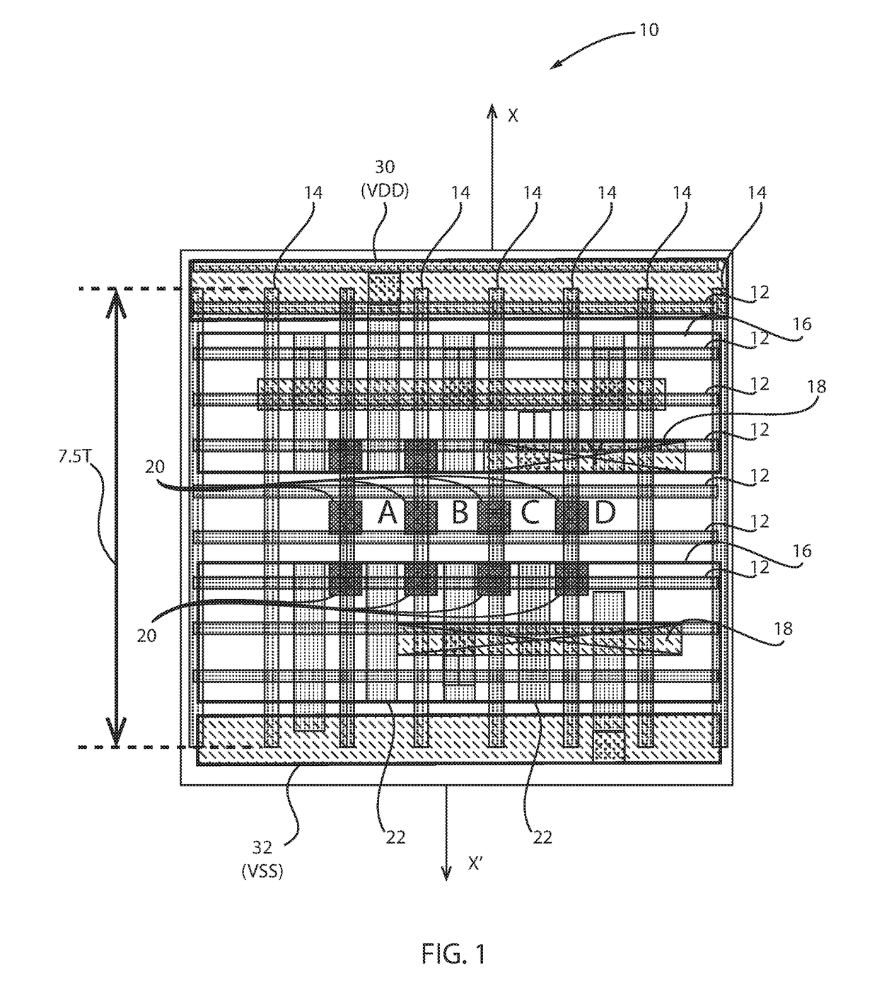
Figure 2 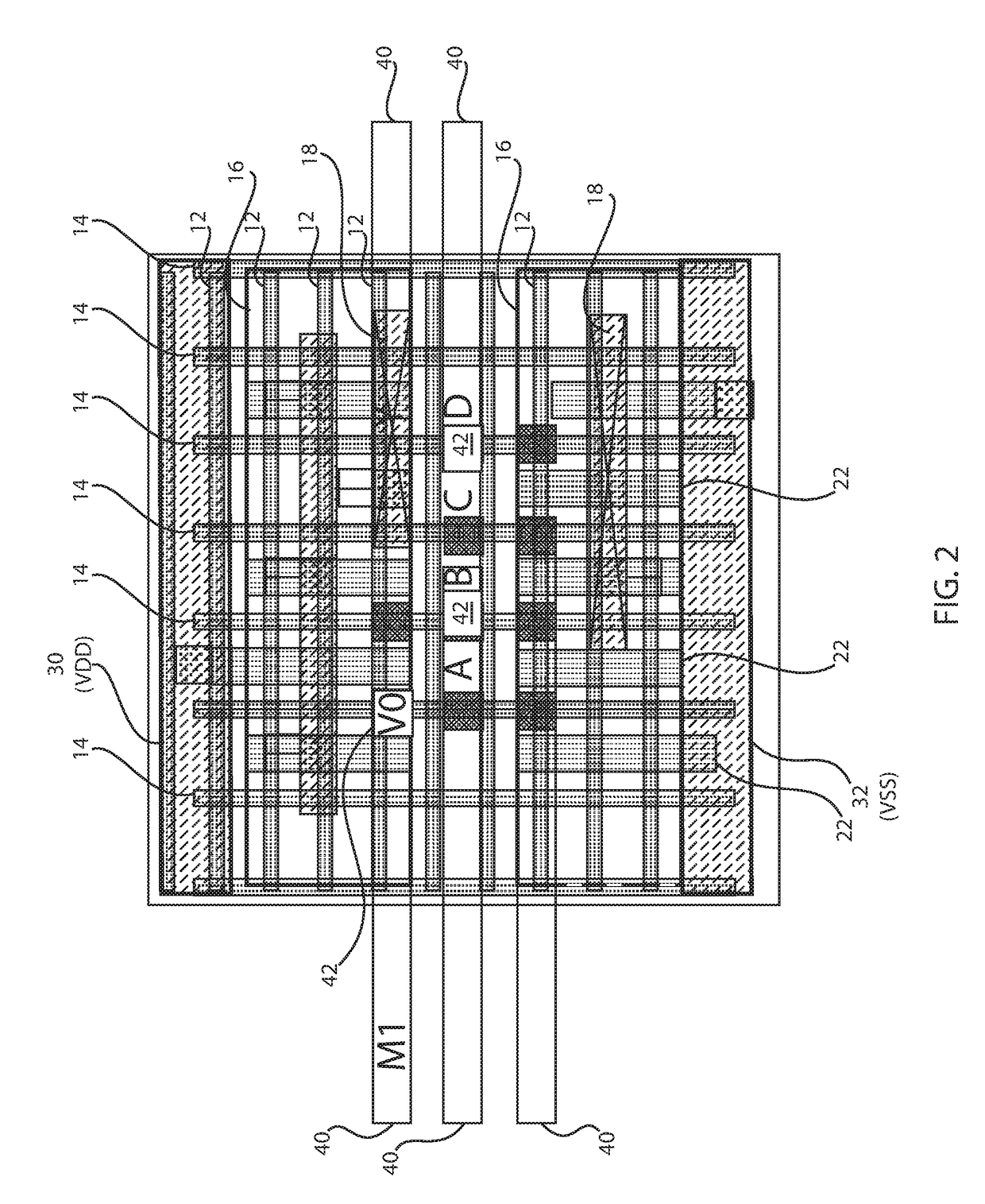
Figure 3
Abstract
Description
BACKGROUNDTechnical Field
[0001] The present invention relates generally to semiconductor devices, and more specifically, to structures and methods of fabricating semiconductor devices using standard semiconductor cell fabrication.Description of the Related Art
[0002] Standard semiconductor cell fabrication is a method for designing integrated circuits (ICs) for specific applications. Circuits are designed based on the desired functions using cells from a cell library, which are combined and constructed by a placement tool to result in the desired circuits. Standard semiconductor cell library performance is limited by the current a transistor of a cell can deliver. This is proportional to the width of the transistor. Thus, it is desirable to enable the transistor to be as wide as possible in a standard cell to deliver high performance circuits.
[0003] Standard cell methodology is a technique of designing ICs with a focus on the logic functions used in the IC. A standard cell includes mult...
Examples
Embodiment Construction
[0031]In accordance with an embodiment, a method is provided for forming a layout of a standard cell. The method includes forming a plurality of gate conductors, forming a plurality of active areas, and forming at least one gate contact (CB contact) within an active region of the plurality of active regions.
[0032]In accordance with another embodiment, a layout of a standard cell is provided. The layout of the standard cell includes a plurality of gate conductors, a plurality of active areas, and at least one gate contact (CB contact) formed within an active region of the plurality of active regions.
[0033]In one or more embodiments, a new and useful logic standard cell architecture is presented that advantageously leverages gate contacts over active regions to reduce the number of metals used while improving pin access. In addition, effective device width (i.e., number of fins) can be maximized to improve performance. AUXFIN is also introduced as a complete and useful design solution...