
Optical element and manufacturing method therefor
a manufacturing method and technology of optical elements, applied in the field of optical elements, can solve the problems of uneven brightness, marked degradation at the position, and the work function of optical elements may vary, so as to prolong the life of optical elements, suppress or eliminate the deterioration variation of optical elements, and suppress the luminance variation of optical elements
Patent Information
- Authority / Receiving Office
- US · United States
- Patent Type
- Patents(United States)
- Current Assignee / Owner
- Publication Date
- 2006-03-07
- Estimated Expiration
- Not applicable · inactive patent
Smart Images
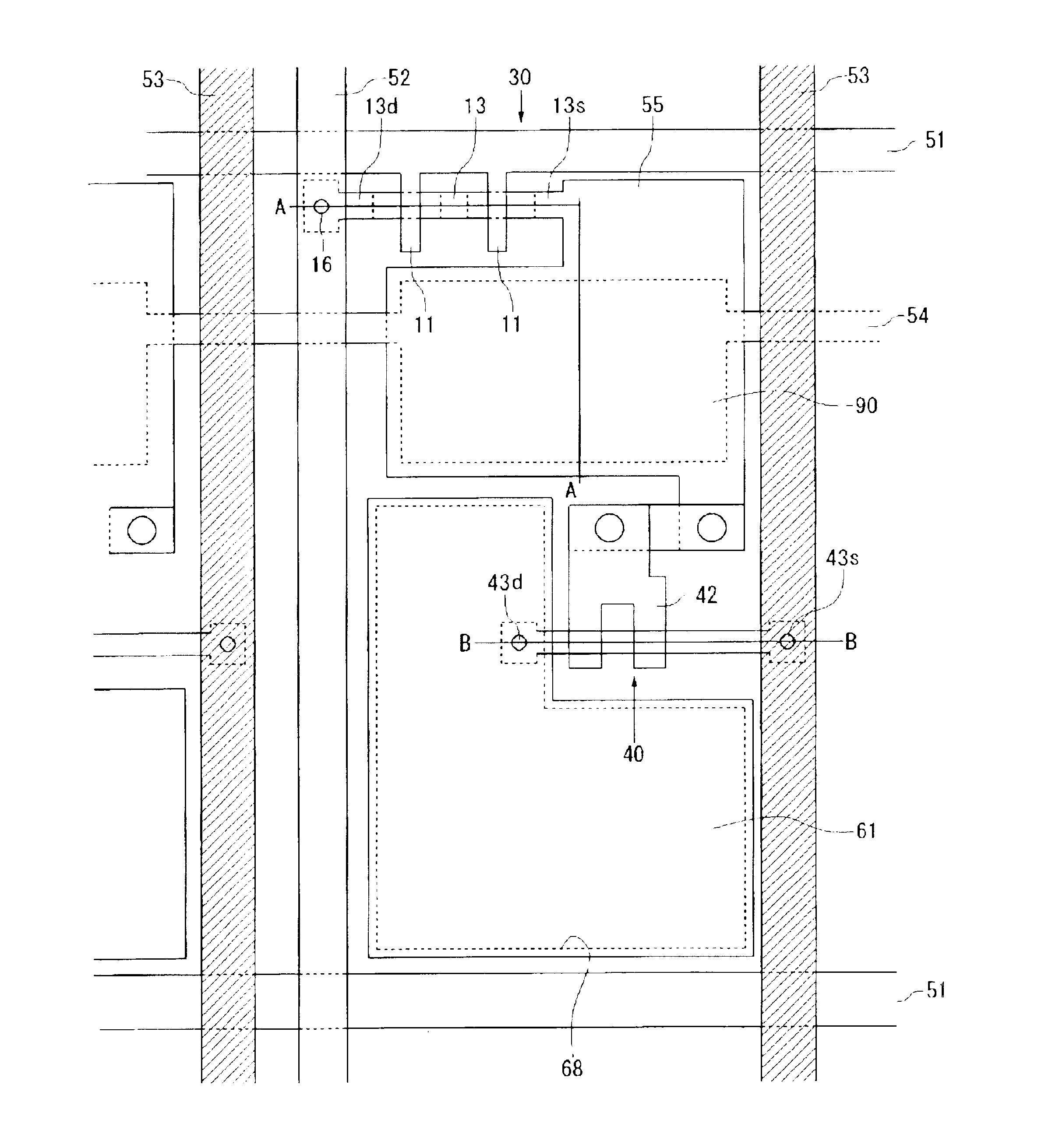
Figure 1 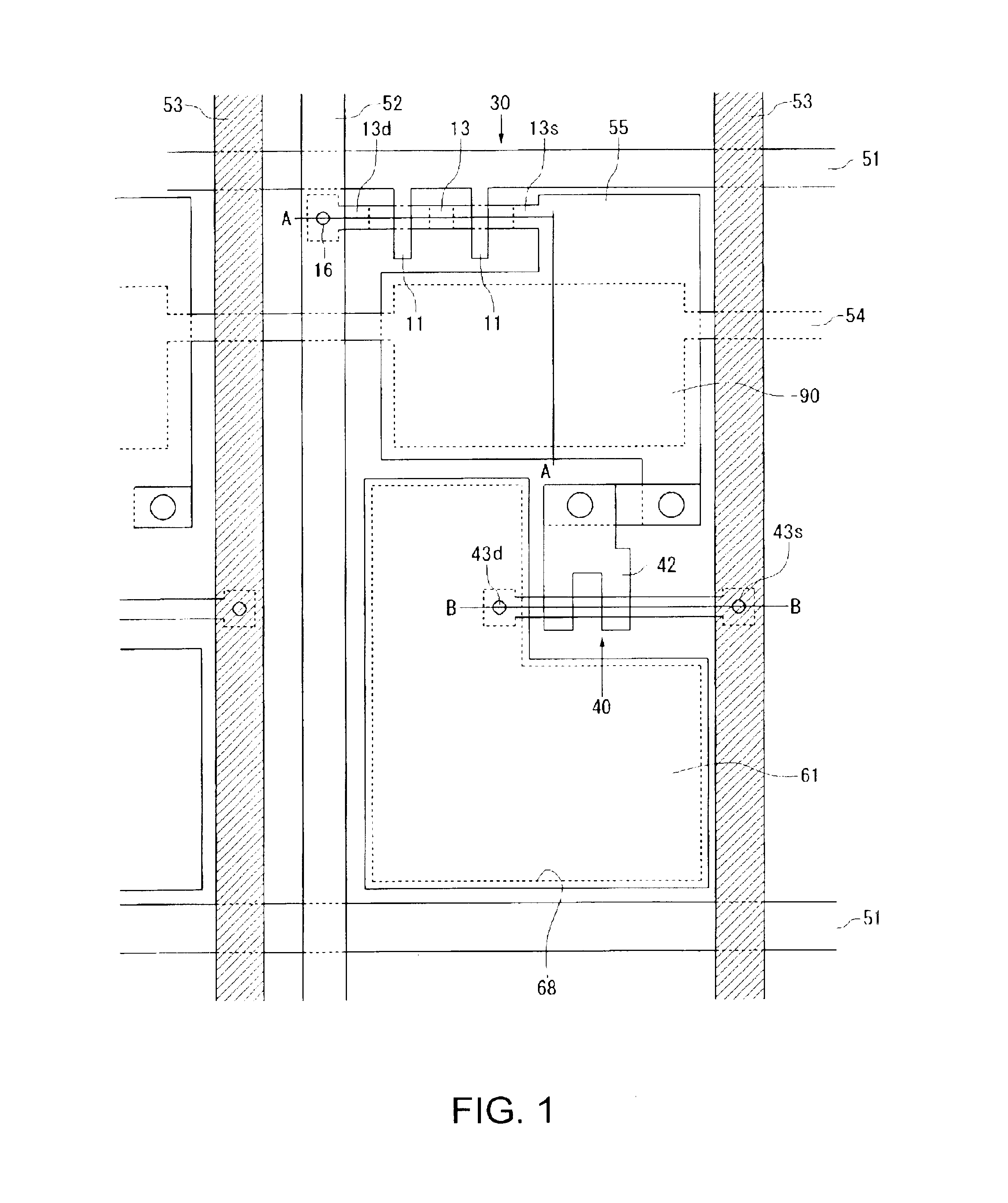
Figure 2 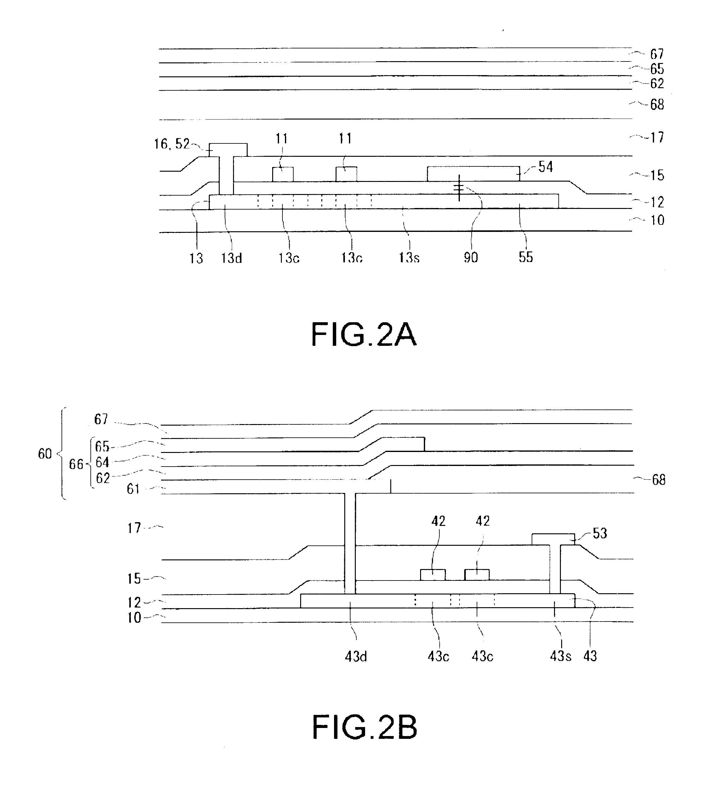
Figure 3
Abstract
Description
BACKGROUND OF THE INVENTION
[0001] 1. Field of the Invention
[0002] The present invention relates to optical elements and a method of manufacturing the optical elements.
[0003] 2. Description of the Related Art
[0004] Recently, organic electroluminescent (EL) display apparatus employing organic light emitting diodes (hereinafter referred to as OLED) as luminous elements are attracting much attention as display apparatus to replace CRTs and LCDs.
[0005] Holes and electrons are injected to a luminescent layer from an anode formed on a glass substrate and a cathode provided above the anode, respectively. Then, these holes and electrons recombine with each other so as to produce excitons. And in the process of radiation deactivation of the excitons, light emanates from the luminescent layer and the organic EL element thus emits the light. It is to be noted here that a hole transport layer is provided between the anode and the luminescent layer whereas an electron transport layer is provided betwe...
Examples
example
[0054]An example of method of forming of the cathode 67 will be described hereinbelow.
[0055]A substrate with an electron transport layer 65 formed thereon was introduced into a chamber, where the ambience was brought into a reduced pressure of 5×10⁻⁵ Pa by a load-lock type cryopump. In this low pressure ambience, lithium fluoride was vapor-deposited in a 1 nm-thick film on the electron transport layer 65. While maintaining this reduced pressure condition, aluminum was vapor-deposited into a 400 nm thickness on the lithium fluoride film at 30° C. The aluminum used was of high purity (99.9% or above).
[0056]Thereafter, the substrate was heat-treated at 80° C. for 60 minutes without being exposed to atmospheric air. This step is a preprocessing for the sealing, with metal or glass, of a cathode side of the entire organic EL display together with desiccant after the formation of the cathode.
[0057]The thickness of the lithium fluoride film can be achieved in the rage of 0.5 nm to 2 nm, bo...