
Field programmable gate array
a gate array and field technology, applied in the field of efficient implementation of dsp functions, can solve the problems of inconvenient fixed inflexible hardware architecture of dsp processors, and limited performance of dsp processors, so as to achieve efficient cascade and waste clock cycles.
Patent Information
- Authority / Receiving Office
- US · United States
- Patent Type
- Patents(United States)
- Current Assignee / Owner
- Publication Date
- 2012-02-07
Smart Images
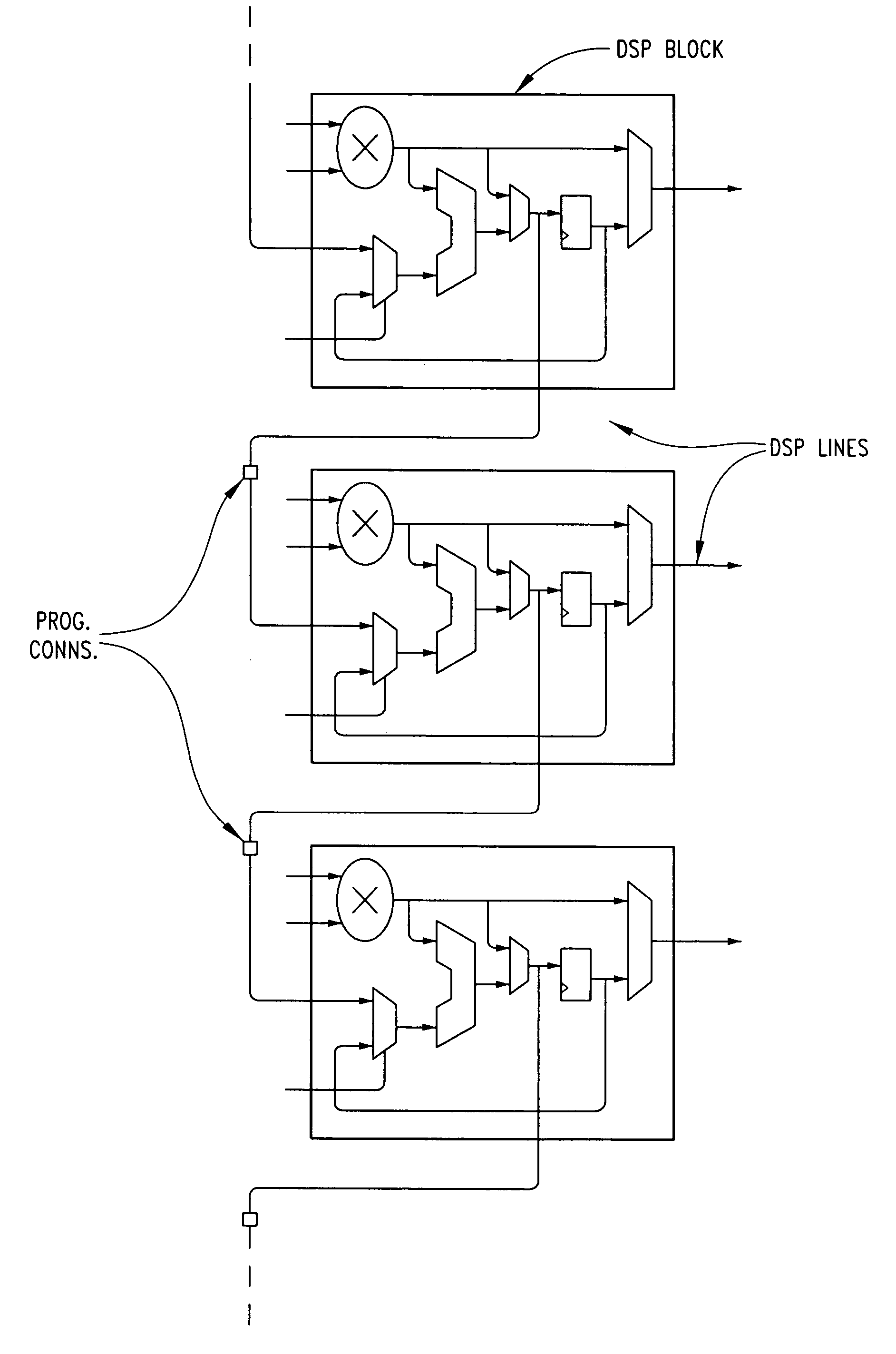
Figure 1 
Figure 2 
Figure 3
Abstract
Description
BACKGROUND OF THE INVENTION
[0001] 1. Field of the Invention
[0002] The present invention relates to an efficient implementation of DSP functions in a field programmable gate array (FPGA).
[0003] 2. Description of the Related Art
[0004] Digital signal processing (DSP) has traditionally been done using enhanced microprocessors. Although DSP processors are programmable through software, yet the DSP processor hardware architecture used is not flexible. Therefore, the performance of the DSP processors is limited by fixed hardware architecture such as bus performance bottlenecks, a fixed number of multiply accumulate (MAC) blocks, fixed memory, fixed hardware accelerator blocks, and fixed data widths. Further the DSP processor's fixed hardware architecture is not suitable for certain applications that might require customized DSP function implementations.
[0005] FPGAs, on the other hand, can provide a fast, cost effective solution to many of today's complex demands for implementing DSP functionali...
Examples
Embodiment Construction
[0050]Embodiments of the present invention are described below with an 18×18 multiplier, a 2:1 multiplexer, and accumulators as an example to aid better understanding. The invention is however not restricted by the sizes shown in any of the figures and any person skilled in the art can very well extend the invention to different sizes or proportions.
[0051]FIG. 3 discloses the proposed architecture of the DSP block containing an 18×18 multiplier (26) followed by an accumulator (28) with the second input of the accumulator (28) either being a feedback or another dynamic input obtained from a multiplexer (27). The register (29) receives its inputs from the accumulator (32) and provides a feedback to the multiplexer (27) as well as provides the final input.
[0052]FIG. 4 discloses an embodiment of the proposed architecture of the DSP block containing an 18×18 multiplier (30) followed by an accumulator (32) with the second input of the accumulator (32) either being a feedback or another dy...