
Semiconductor memory device
a memory device and semiconductor technology, applied in semiconductor devices, digital storage, instruments, etc., can solve the problems of limiting the number of writing operations, high power consumption needed for retaining data during a standby period, and cannot be used in a case where the writing operation is not used, so as to reduce the voltage gap and reduce the power consumption for holding data.
Patent Information
- Authority / Receiving Office
- US · United States
- Patent Type
- Patents(United States)
- Current Assignee / Owner
- Publication Date
- 2015-10-13
- Estimated Expiration
- Not applicable · inactive patent
Smart Images
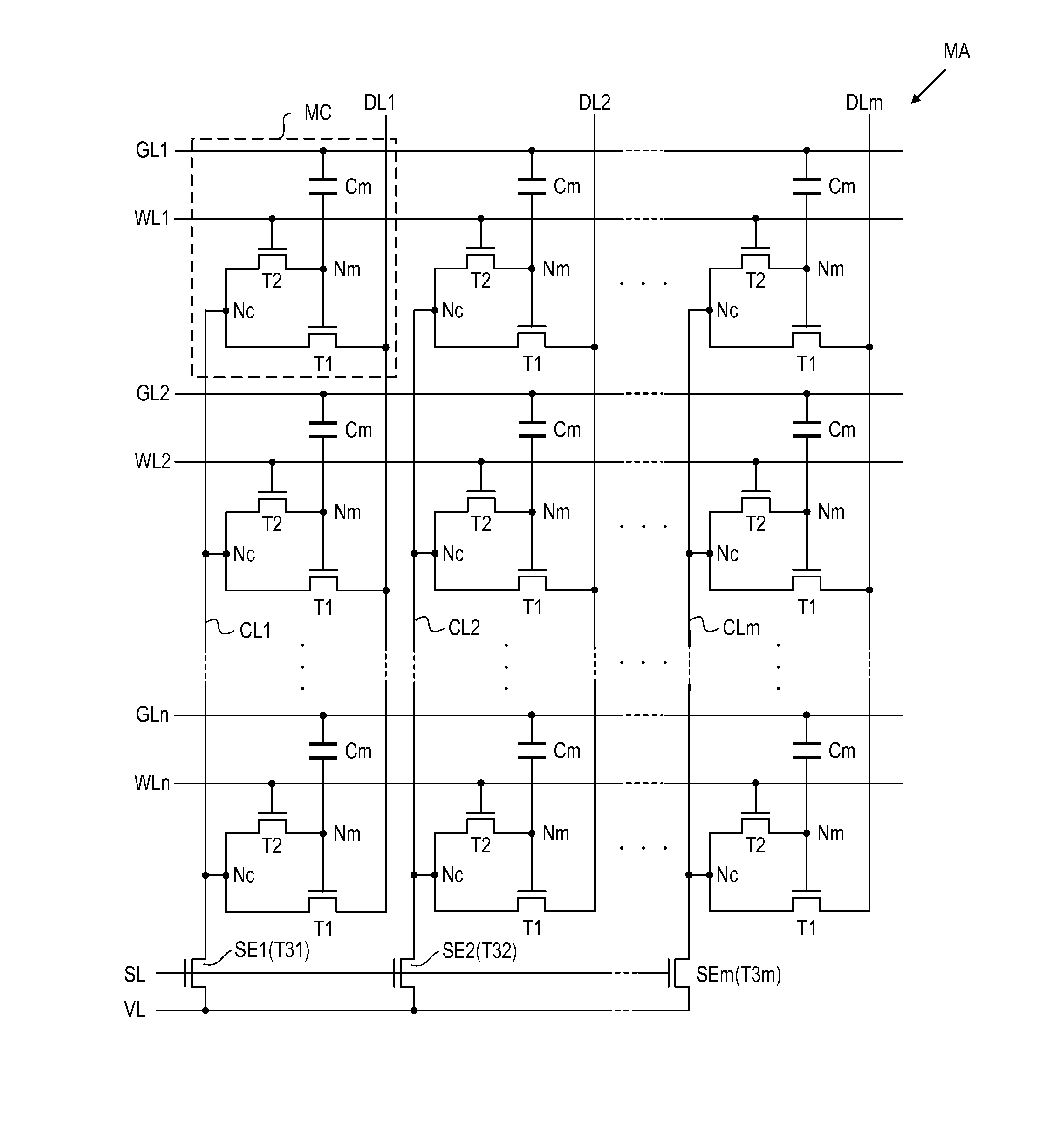
Figure 1 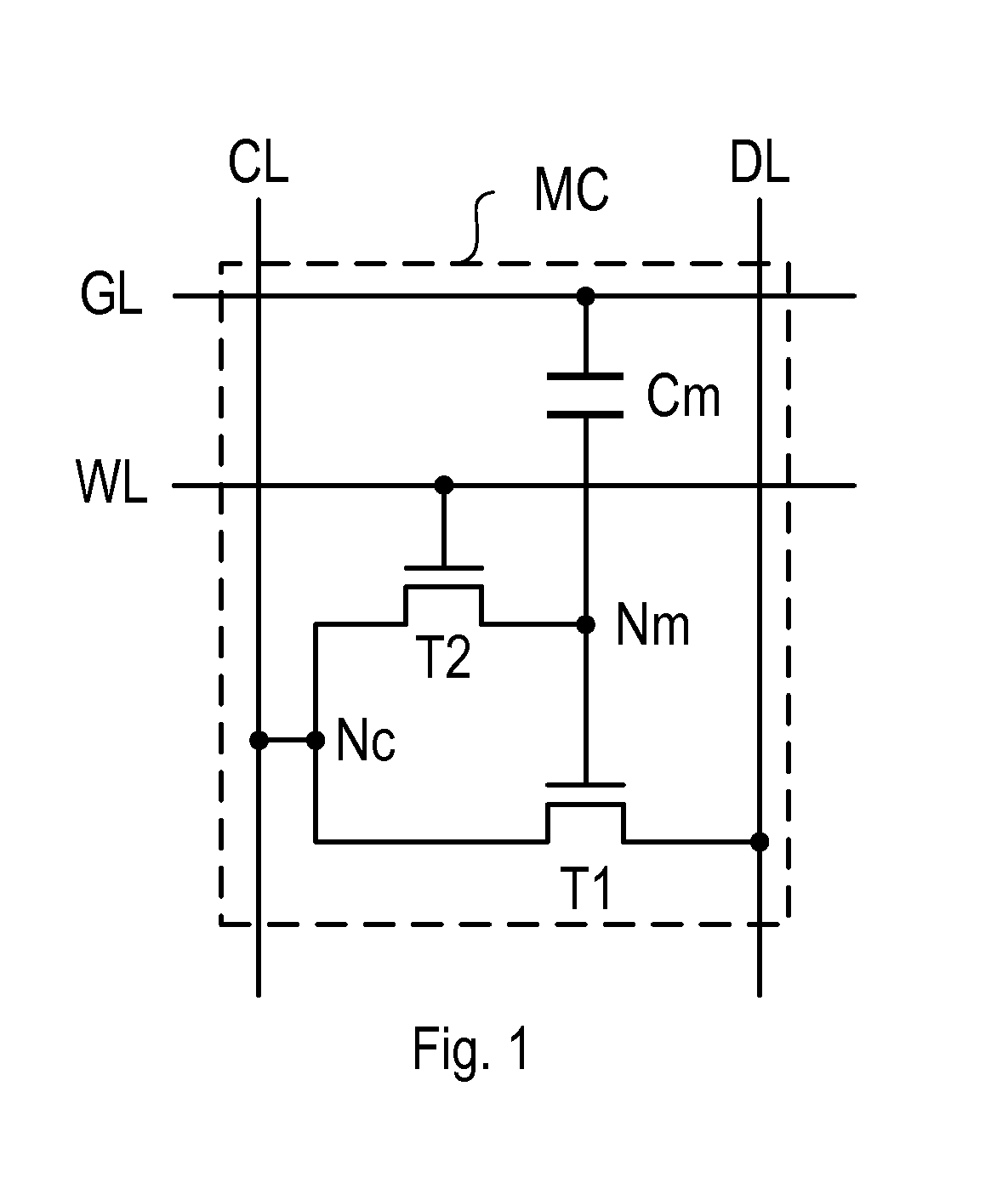
Figure 2 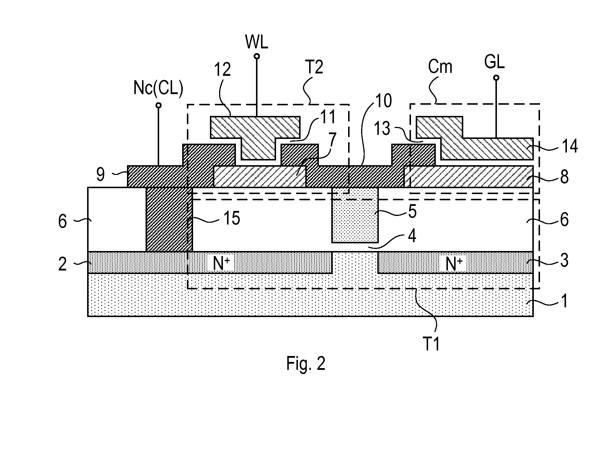
Figure 3
Abstract
Description
CROSS-REFERENCE TO RELATED APPLICATIONS
[0001] This application is a National Phase filing under 35 U.S.C. §371 of International Application No. PCT / JP2013 / 053479 filed on Feb. 14, 2013, and which claims priority to Japanese Patent Application No. 2012-090906 filed on Apr. 12, 2012.TECHNICAL FIELD
[0002] The present invention relates to a semiconductor memory device including an oxide semiconductor insulated gate FET (Field Effect Transistor), and more particularly, to a semiconductor memory device suitable for storing multilevel information.BACKGROUND ART
[0003] The semiconductor memory device is broadly divided into a RAM (Random Access Memory) and a ROM (Read Only Memory). As for the RAM, there is no limit on the number of writing operations, but it has the problem that retained data is lost at the time of power-supply disconnection, so that high power consumption is needed for retaining data during a standby period. Meanwhile, as for the ROM, data can be retained at the time of power-...
Examples
first embodiment
[0047]In the first embodiment, a description will be given to a semiconductor memory device in the present invention (hereinafter, simply referred to as the memory device), and a circuit configuration of a memory cell used in the memory device.
[0048]FIG. 1 shows an equivalent circuit diagram of a memory cell MC. The memory cell MC is provided with a first transistor element T1 composed of an insulated gate FET, a second transistor element T2 composed of an oxide semiconductor insulated gate FET, and a capacitive element Cm. In this embodiment, it is assumed that the first transistor element T1 is an n-channel MOSFET formed on a silicon substrate, and the second transistor element T2 is an n-channel thin film transistor (TFT).
[0049]In addition, as shown in FIG. 1, in the memory cell MC, a memory node Nm is formed at a connection point of a gate electrode of the first transistor element T1, a source electrode of the second transistor element T2, and one end of the capacitive element C...
second embodiment
[0071]In the second embodiment, a detailed description will be given to the initialization operation, the writing operation, and the reading operation, for the memory cell array MA, in accordance with the circuit configuration of the memory cell MC, the memory cell array MA, and the memory device 20 described in the first embodiment. In the following description, it is assumed that a plurality of bits of the input data inputted as the data input signal DIN are divided to every two bits, and one of four-value data (0 to 3) each having the two bits is written in the one memory cell MC, and one of the four-value data written in each memory cell MC is read. In addition, according to this embodiment, the voltage state of the memory node Nm which has been initialized in the initialization operation is allocated to the one data value “3” in the four-value data, but the initialized voltage state is not necessarily allocated to the one data value.
[0072]In addition, in the following descripti...
third embodiment
[0121]The description has been given to the reading operation in the case where the reading circuit 26 is the voltage detection type sense amplifier in the second embodiment, but in the third embodiment, a description will be given to the reading operation in the case where the reading circuit 26 is the current detection type sense amplifier, with reference to FIGS. 9A to 9C and 10. The initialization operation and the writing operation are the same as descried in the second embodiment. FIG. 10 shows a timing chart in a case where the reading operation is performed for the one selected row after the writing operation has been performed, by selecting one or more data lines DL in the same manner as in FIG. 8. FIGS. 9A to 9C are also applied to the case where the reading circuit 26 is the current detection type sense amplifier.
[0122]In the case where the reading circuit 26 is the current detection type sense amplifier, a voltage condition applied to each signal line is the same as that...