
Electronic device, electronic apparatus, and method of manufacturing electronic device
a technology of electronic equipment and electronic components, applied in the field of electronic equipment and electronic equipment manufacturing, can solve the problems of significantly affecting the yield ratio, dramatic deformation of the yield ratio, and degradation of the reliability of the functional element, so as to achieve the effect of reducing the size and space of the devi
Patent Information
- Authority / Receiving Office
- US · United States
- Patent Type
- Patents(United States)
- Current Assignee / Owner
- Publication Date
- 2016-12-13
Smart Images
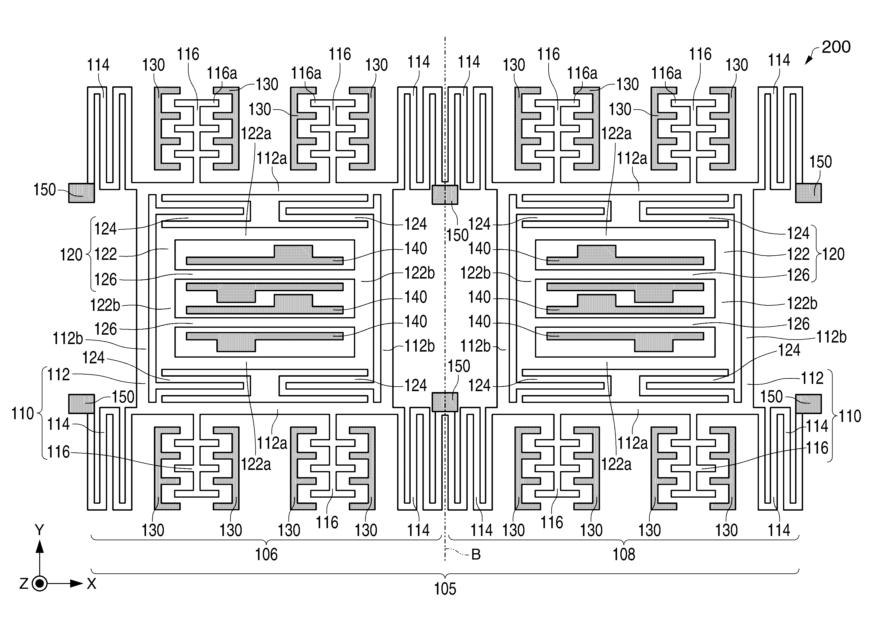
Figure 1 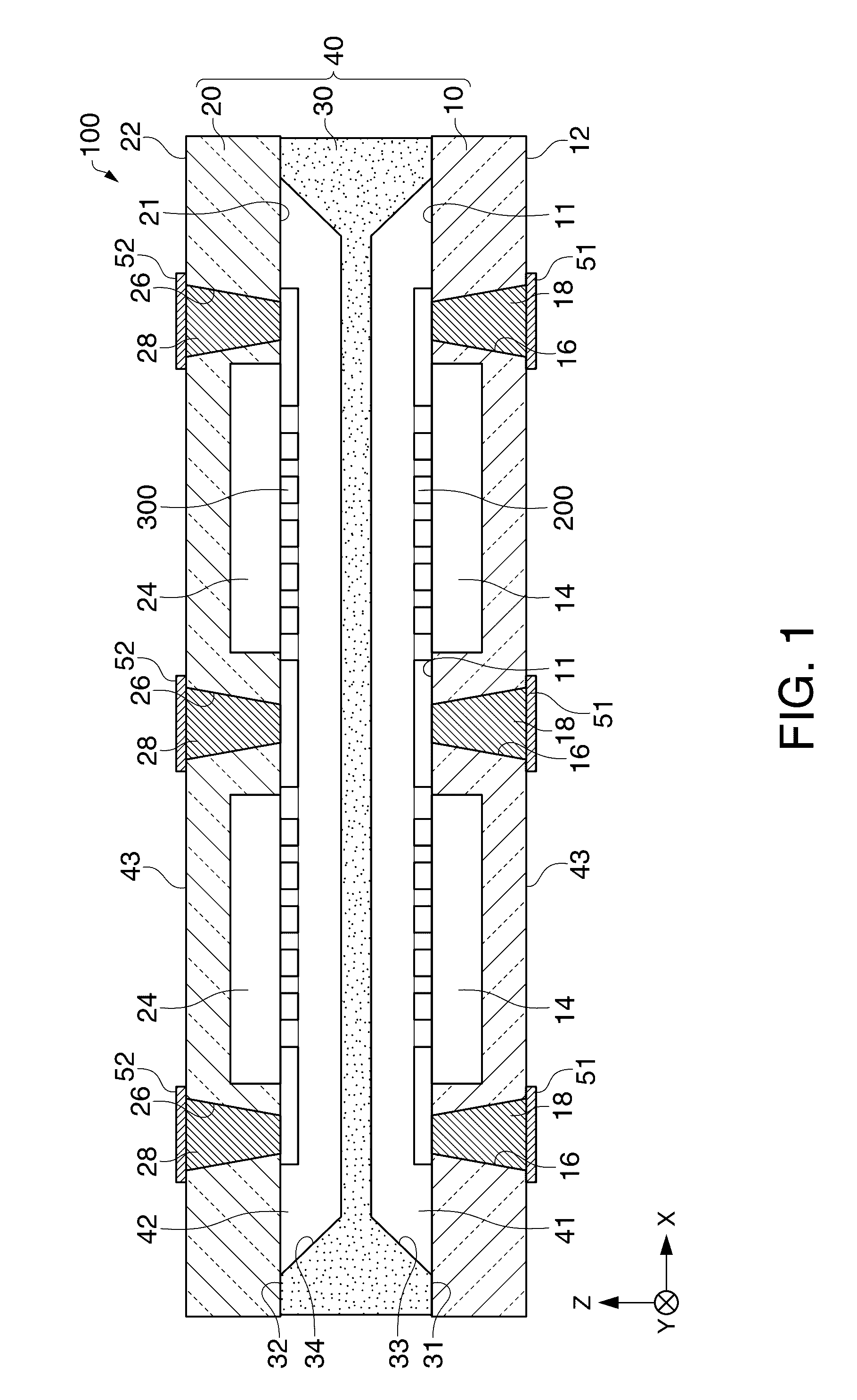
Figure 2 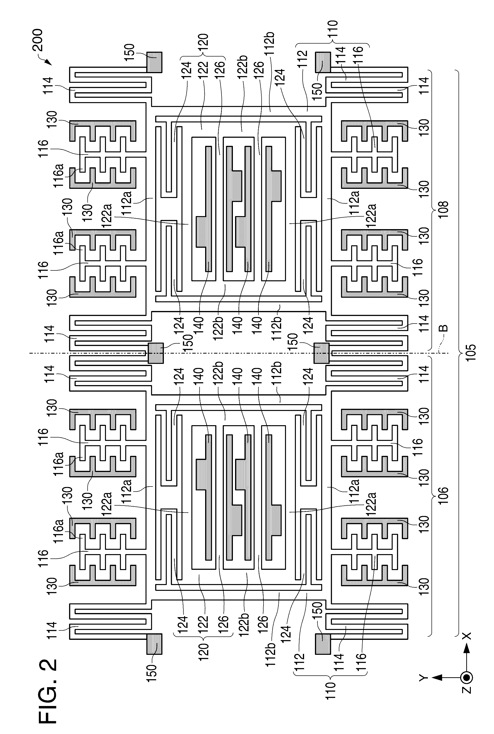
Figure 3
Abstract
Description
BACKGROUND
[0001] 1. Technical Field
[0002] The present invention relates to an electronic device, an electronic apparatus, and a method of manufacturing the electronic device.
[0003] 2. Related Art
[0004] In recent years, there have been developed an electronic device such as an inertia sensor for detecting a physical quantity using, for example, a silicon MEMS (micro-electromechanical system) technology. Such an electronic device is used for, for example, a camera-shake correction function of a digital still camera (DSC), a car navigation system, and an action input device in a game machine.
[0005] In the field of such an electronic device, there is a demand for miniaturization and space saving of the device. For example, JP-A-2002-5950 discloses an electronic device (a composite element sensor) provided with, for example, an angular velocity sensor and an acceleration sensor disposed on the same substrate.SUMMARY
[0006] An advantage of some aspects of the invention is to provide an electroni...
Examples
first embodiment
1.1. First Embodiment
[0070]Firstly, an electronic device according to a first embodiment will be explained with reference to the accompanying drawings. FIG. 1 is a cross-sectional view schematically showing an electronic device 100 according to the first embodiment. For the sake of convenience, in the drawing, the X axis, the Y axis, and the Z axis are shown as the three axes perpendicular to each other.
[0071]As shown in FIG. 1, the electronic device 100 includes a first cavity 41 composed of a first base body 10, a second base body 20, and a third base body 30, a package 40 having a second cavity 42, and first and second functional elements 200, 300 housed in the package 40. It should be noted that, for the sake of convenience, the first and second functional elements 200, 300 are simplified in FIG. 1.
[0072]The electronic device 100 is a composite element sensor having a plurality of physical quantity detection sensors mounted in the same package (the same substrate). The first and...
first modified example
[0141]Then, a first modified example of the first embodiment will be explained with reference to FIG. 8. FIG. 8 is a cross-sectional view schematically showing an electronic device 101 according to the first modified example. The electronic device 101 according to the first modified example is different from the electronic device 100 according to the first embodiment in the shapes of the first base body 10, the second base body 20, and the third base body 30. In the following description, only the points in which the electronic device 101 is different from the electronic device 100 according to the first embodiment will be explained. The members having already been explained will be denoted with the same reference symbols, and the detailed explanation thereof will be omitted.
[0142]As shown in the drawing, in the electronic device 101 according to the first modified example, the third base body 30 is not provided with the first recessed section 33 and the second recessed section 34, ...
second modified example
[0146]Then, a second modified example of the first embodiment will be explained with reference to FIG. 9. FIG. 9 is a cross-sectional view schematically showing an electronic device 102 according to the second modified example. The electronic device 102 according to the second modified example is different from the electronic device 100 according to the first embodiment in the shape of a third base body 330. In the following description, only the points in which the electronic device 102 is different from the electronic device 100 according to the first embodiment will be explained. The members having already been explained will be denoted with the same reference symbols, and the detailed explanation thereof will be omitted.
[0147]As shown in the drawing, in the electronic device 102 according to the second modified example, the third base body 330 is not provided with the first recessed section 33 and the second recessed section 34, but is provided with an opening section 331 for co...