Advancements in Hall Effect Sensor Technology for Precision Tasks
SEP 22, 202510 MIN READ
Generate Your Research Report Instantly with AI Agent
PatSnap Eureka helps you evaluate technical feasibility & market potential.
Hall Effect Sensor Evolution and Objectives
Hall Effect sensors have evolved significantly since their discovery by Edwin Hall in 1879. Initially, these sensors were primarily laboratory instruments with limited practical applications. The fundamental breakthrough came in the 1950s with the development of semiconductor technology, which enabled the miniaturization and integration of Hall Effect sensors into practical devices. By the 1970s, these sensors began appearing in industrial applications, primarily for proximity detection and simple position sensing.
The 1980s and 1990s marked a period of rapid advancement with the introduction of integrated circuit technology, allowing Hall Effect sensors to be combined with signal processing capabilities on a single chip. This integration dramatically improved sensitivity, reliability, and reduced form factors, opening new application domains in automotive systems, consumer electronics, and industrial automation.
The early 2000s witnessed further refinement with the emergence of digital Hall Effect sensors, offering improved signal-to-noise ratios and programmable features. These advancements enabled more precise measurements and expanded the operational temperature range, making the sensors suitable for harsh environments.
Recent technological trends have focused on enhancing sensitivity and precision through innovative materials and designs. The introduction of vertical Hall Effect sensors has enabled three-dimensional magnetic field sensing, while advances in materials science have produced sensors capable of detecting extremely weak magnetic fields. Modern Hall Effect sensors now incorporate sophisticated compensation algorithms to mitigate temperature drift and other environmental factors that previously limited measurement accuracy.
The current trajectory points toward intelligent sensor systems with integrated machine learning capabilities for adaptive calibration and predictive maintenance. Miniaturization continues to push boundaries, with some sensors now approaching nanoscale dimensions, enabling integration into increasingly compact devices and systems.
The primary objectives for advancing Hall Effect sensor technology include achieving sub-microtesla sensitivity for precision tasks, developing sensors with enhanced stability across wider temperature ranges, and reducing power consumption for battery-operated and energy-harvesting applications. There is also a strong focus on improving response times to enable real-time control systems in high-speed applications.
Additional objectives include enhancing immunity to electromagnetic interference, developing self-calibrating sensors to maintain accuracy over extended operational lifetimes, and creating more robust packaging solutions for deployment in extreme environments. The integration of wireless communication capabilities represents another key goal, enabling seamless incorporation into IoT ecosystems and facilitating remote monitoring and control applications.
Market Analysis for Precision Sensing Applications
The global market for precision sensing applications utilizing Hall Effect sensor technology is experiencing robust growth, driven by increasing demand for high-precision measurement solutions across multiple industries. Current market valuations place the precision Hall Effect sensor segment at approximately 2.1 billion USD in 2023, with projections indicating a compound annual growth rate of 7.8% through 2028. This growth trajectory significantly outpaces the broader sensor market, reflecting the expanding application scope of advanced Hall Effect technologies.
Automotive applications currently represent the largest market segment, accounting for roughly 38% of total demand. The transition toward electric vehicles and advanced driver assistance systems (ADAS) has dramatically increased requirements for precise position sensing, current monitoring, and rotational speed measurement. Automotive manufacturers are increasingly adopting high-precision Hall sensors capable of operating reliably in harsh environments while maintaining measurement accuracy within the 0.1% range.
Industrial automation constitutes the second-largest market segment at approximately 27%, with particular growth in robotics and smart manufacturing systems. The Industry 4.0 paradigm has elevated requirements for sensor precision, reliability, and integration capabilities, creating substantial opportunities for advanced Hall Effect technologies. Notably, demand for sensors capable of sub-micron positioning accuracy has grown by over 15% annually in this sector.
Consumer electronics represents a rapidly expanding application area, currently comprising about 18% of the market but growing at nearly 10% annually. Smartphones, wearables, and smart home devices increasingly incorporate Hall Effect sensors for precise gesture recognition, position sensing, and power management functions. The miniaturization trend in this sector has driven development of ultra-compact Hall sensors with dimensions below 1.0 × 1.0 mm while maintaining high sensitivity.
Healthcare applications, though currently representing only 8% of the market, show the highest growth potential at 12% annually. Medical devices requiring precise positioning, fluid flow measurement, and non-invasive monitoring are increasingly adopting Hall Effect technology for its reliability and accuracy advantages over alternative sensing methods.
Regional analysis reveals Asia-Pacific as the dominant market, accounting for approximately 42% of global demand, followed by North America (28%) and Europe (23%). China and South Korea are experiencing particularly rapid growth rates, driven by their expanding electronics manufacturing and automotive sectors. The North American market shows strong demand in aerospace and defense applications, while European consumption is heavily influenced by premium automotive and industrial automation requirements.
Current Limitations and Technical Barriers
Despite significant advancements in Hall effect sensor technology, several technical barriers continue to limit their application in high-precision tasks. The primary limitation remains the inherent signal-to-noise ratio (SNR) challenges, particularly in environments with electromagnetic interference. Current Hall sensors typically achieve resolution limits of 10-100 μT, which proves insufficient for ultra-precision applications in quantum computing and advanced medical diagnostics where nano-Tesla sensitivity is required.
Temperature dependency presents another significant barrier, with most commercial Hall sensors exhibiting drift coefficients of 100-500 ppm/°C. This thermal instability necessitates complex compensation algorithms that increase system complexity and power consumption, making miniaturization difficult for portable applications.
Material constraints further impede advancement, as traditional silicon-based Hall sensors face fundamental physical limitations in sensitivity. While III-V semiconductor compounds like GaAs and InAs offer higher electron mobility, they introduce manufacturing complexity and cost barriers that limit widespread adoption. The integration of these specialized materials with standard CMOS processes remains technically challenging.
Power consumption represents a critical limitation for IoT and wearable applications. Current Hall sensor systems typically require 1-10 mW during operation, which is prohibitive for energy-harvesting or battery-powered devices designed for long-term deployment. The trade-off between sensitivity and power efficiency continues to challenge designers.
Miniaturization efforts face barriers related to packaging technologies. As sensors shrink below 1mm², issues of mechanical stress during packaging increasingly affect measurement accuracy. Current encapsulation techniques introduce stress-induced offset errors that can reach 2-5% of full-scale output, requiring additional calibration steps.
Hysteresis effects and non-linearity issues persist in many Hall sensor designs, with typical non-linearity errors ranging from 0.5% to 2%. These characteristics limit the dynamic range and absolute accuracy achievable in precision applications such as industrial robotics and autonomous navigation systems.
The integration density of Hall sensors in multi-axis configurations faces limitations due to cross-talk effects. Current designs struggle to maintain measurement integrity when sensor elements are placed closer than 0.5mm apart, restricting the development of high-density magnetic field mapping solutions needed for advanced NDT (Non-Destructive Testing) applications.
Response time limitations also hinder applications requiring high-frequency magnetic field detection. Most commercial Hall sensors exhibit bandwidth limitations of 20-100 kHz, insufficient for emerging applications in high-speed motor control and real-time magnetic anomaly detection systems.
State-of-the-Art Hall Effect Sensing Solutions
01 Enhanced Hall sensor design for improved precision
Advanced Hall sensor designs incorporate specialized structures and materials to enhance measurement precision. These designs include optimized semiconductor layers, integrated flux concentrators, and improved electrode configurations that minimize interference and noise. Such enhancements allow for more accurate magnetic field detection and higher resolution sensing capabilities, making them suitable for applications requiring high precision measurements.- Enhanced Hall sensor design for improved precision: Advanced Hall sensor designs incorporate specialized structures and materials to enhance measurement precision. These designs include optimized semiconductor materials, improved magnetic field concentrators, and integrated circuit configurations that minimize noise and interference. Such enhancements allow for more accurate detection of magnetic fields, resulting in higher precision measurements for various applications including position sensing and current monitoring.
- Calibration and compensation techniques: Various calibration and compensation techniques are employed to improve Hall effect sensor precision. These include temperature compensation circuits, offset voltage correction, and digital signal processing algorithms that adjust for environmental variations and manufacturing inconsistencies. Advanced calibration methods can significantly reduce measurement errors and drift, ensuring consistent performance across operating conditions.
- Integration with signal processing systems: Hall effect sensors achieve higher precision through integration with sophisticated signal processing systems. These systems include analog-to-digital converters, amplification circuits, and filtering components that enhance signal quality. Modern implementations may incorporate microprocessors for real-time signal analysis and correction, enabling more accurate magnetic field measurements and improved overall system performance.
- Miniaturization and packaging innovations: Advancements in miniaturization and packaging technologies have led to more precise Hall effect sensors. Reduced sensor size minimizes spatial averaging effects, allowing for more localized and accurate magnetic field measurements. Innovative packaging techniques protect sensitive components from external influences while maintaining precise alignment of sensing elements, resulting in improved measurement stability and reliability.
- Multi-axis and 3D sensing capabilities: Modern Hall effect sensor technology incorporates multi-axis and three-dimensional sensing capabilities to enhance precision. By measuring magnetic fields in multiple directions simultaneously, these sensors provide more comprehensive data for accurate position and orientation determination. Advanced designs include arrays of sensing elements and specialized geometries that enable precise spatial resolution and improved measurement accuracy in complex magnetic environments.
02 Calibration and compensation techniques
Various calibration and compensation techniques are employed to improve Hall sensor precision. These include temperature compensation circuits, offset voltage correction, and digital signal processing algorithms that adjust for environmental variations and manufacturing inconsistencies. Advanced calibration methods can significantly reduce measurement errors and drift, resulting in more stable and accurate sensor performance across varying operating conditions.Expand Specific Solutions03 Integration with complementary technologies
Hall effect sensors achieve higher precision when integrated with complementary technologies such as amplification circuits, filtering systems, and digital interfaces. These integrated solutions combine the Hall sensing element with signal conditioning components on a single chip, reducing noise and interference while improving signal quality. The integration enables more precise magnetic field measurements and facilitates easier implementation in various applications.Expand Specific Solutions04 Specialized Hall sensors for high-precision applications
Specialized Hall sensor designs cater to high-precision applications such as current sensing, position detection, and rotation measurement. These sensors feature optimized geometries, specialized materials, and application-specific integrated circuits that enhance their precision for particular use cases. The specialized designs may include vertical Hall sensors, spinning current techniques, or custom sensing elements tailored to specific measurement requirements.Expand Specific Solutions05 Noise reduction and signal enhancement methods
Various techniques are employed to reduce noise and enhance signal quality in Hall effect sensors, directly improving measurement precision. These include chopper stabilization, differential sensing arrangements, and advanced shielding designs. Additional methods involve specialized packaging to minimize external interference, dynamic offset cancellation circuits, and improved power management systems that reduce thermal noise and other disturbances affecting sensor accuracy.Expand Specific Solutions
Leading Manufacturers and Competitive Landscape
Hall Effect sensor technology for precision tasks is currently in a mature growth phase, with the market expected to reach $2.5 billion by 2026. The competitive landscape features established players like Infineon Technologies, Honeywell, and Allegro MicroSystems dominating with advanced sensing solutions, while STMicroelectronics and Texas Instruments are rapidly expanding their market share through innovative product offerings. The technology has evolved from basic position sensing to sophisticated applications in automotive, industrial automation, and consumer electronics, with recent advancements focusing on improved sensitivity, miniaturization, and integration with IoT systems. Companies like Bosch and TDK-Micronas are driving innovation in high-precision applications, while emerging players from Asia are challenging incumbents with cost-effective solutions for growing markets.
Honeywell International Technologies Ltd.
Technical Solution: Honeywell has developed sophisticated Hall Effect sensor technology through their SS360/SS460 series and SMART position sensors. Their approach combines proprietary integrated circuits with advanced packaging techniques to create highly reliable sensors for extreme environments. Honeywell's Hall Effect sensors incorporate patented chopper stabilization techniques that virtually eliminate temperature-induced drift and magnetic offsets, achieving stability across temperatures from -40°C to +150°C. Their SMART position sensors utilize multiple Hall elements arranged in proprietary configurations to enable non-contact measurement of rotary and linear position with accuracy better than 0.1% of full scale. Honeywell has pioneered the integration of digital signal processing directly within the sensor housing, enabling advanced features such as programmable thresholds, hysteresis control, and self-diagnostics. Their latest innovations include sensors with integrated ASIC technology that provides linearized analog or digital outputs (PWM, I2C, SPI) while maintaining immunity to external electromagnetic interference through specialized shielding techniques and differential sensing architectures.
Strengths: Exceptional durability and reliability in harsh environments (vibration, shock, contaminants); industry-leading temperature stability; comprehensive EMI/RFI protection ensures measurement integrity in noisy environments. Weaknesses: Higher cost structure compared to commodity Hall sensors; larger physical footprint for some specialized sensor packages; longer lead times for customized solutions.
Texas Instruments Incorporated
Technical Solution: Texas Instruments has developed advanced Hall Effect sensor technology through their DRV5x series and TMAG5x family of sensors. Their approach integrates high-precision Hall elements with sophisticated analog front-end circuitry and digital signal processing capabilities. TI's Hall sensors feature chopper-stabilized amplifiers and dynamic offset cancellation techniques that reduce measurement errors to less than 2% across the operating temperature range. Their TMAG5170 3D Hall Effect sensor achieves industry-leading resolution of 0.45mT with a sampling rate up to 20kHz, enabling precise position and rotation sensing in demanding applications. TI has pioneered the integration of temperature sensors, ADCs, and programmable gain amplifiers within their Hall sensor packages, creating complete measurement systems with minimal external components. Their latest innovations include ultra-low-power Hall sensors that consume less than 1.5μA in sleep mode while maintaining rapid wake-up capabilities for battery-powered applications. TI's sensors also feature advanced diagnostic functions with programmable thresholds and interrupt capabilities that simplify system integration and improve reliability.
Strengths: Exceptional power efficiency makes them ideal for battery-powered applications; comprehensive integration reduces BOM costs and simplifies system design; excellent EMI immunity through advanced circuit techniques. Weaknesses: More limited operating temperature range compared to some specialized competitors; fewer packaging options for extreme environments; less extensive automotive qualification portfolio.
Key Patents and Technical Innovations
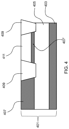
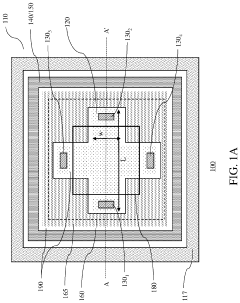
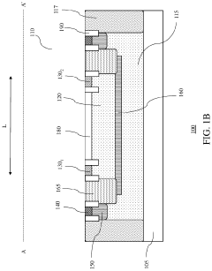
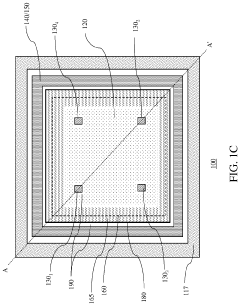
Hall effect sensor with enhanced sensitivity and method for producing the same
PatentActiveUS10707408B2
Innovation
- A Hall effect sensor is formed with a thin Hall plate and optional front and back gates, and reduced or omitted doping to enhance sensitivity, using a silicon-on-insulator (SOI) substrate with shallow trench isolation (STI) structures and N+ dopant ion implantation to create N+ implantation regions.
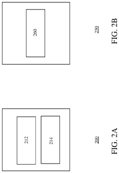
Hall effect sensors with tunable sensitivity and/or resistance
PatentActiveUS20200292631A1
Innovation
- A Hall effect sensor design with a tunable Hall plate thickness, achieved through adjustable implants in the separation layer and bias voltage applied to the separation layer, allowing for customizable current sensitivity and resistance, enabling high voltage and current sensitivity within the same device.
Material Science Impacts on Sensor Performance
Material science advancements have fundamentally transformed Hall effect sensor technology, enabling unprecedented levels of precision and reliability. The semiconductor materials used in sensor fabrication directly influence key performance parameters including sensitivity, temperature stability, and signal-to-noise ratio. Traditional silicon-based Hall sensors are increasingly being complemented or replaced by compound semiconductor materials such as gallium arsenide (GaAs), indium antimonide (InSb), and indium arsenide (InAs), which offer superior electron mobility characteristics.
Recent breakthroughs in thin-film deposition techniques have allowed for the creation of ultra-thin sensing elements with enhanced sensitivity. Particularly noteworthy is the development of graphene-based Hall sensors, where the two-dimensional carbon structure exhibits exceptional electron mobility at room temperature, resulting in significantly improved magnetic field detection capabilities. These graphene sensors demonstrate up to 30 times higher sensitivity compared to conventional silicon alternatives while maintaining stability across wider temperature ranges.
Nanomaterial integration represents another frontier in Hall sensor development. Magnetic nanoparticles and nanowires incorporated into sensing elements create localized field enhancement effects, effectively amplifying weak magnetic signals. This innovation has proven especially valuable in biomedical applications where minute magnetic field detection is essential for diagnostic procedures.
The emergence of flexible substrate materials has enabled conformable Hall sensors that can adapt to non-planar surfaces while maintaining measurement accuracy. Polyimide and other polymer substrates combined with specialized deposition techniques allow sensors to be integrated into previously inaccessible locations, expanding application possibilities in robotics and wearable technology sectors.
Temperature compensation mechanisms have been revolutionized through material science innovations. Multi-layer structures incorporating materials with opposing temperature coefficients effectively neutralize thermal drift, a historical limitation of Hall effect sensors. These composite structures maintain calibration accuracy across operating temperatures from -40°C to +150°C, critical for automotive and industrial applications where environmental conditions fluctuate dramatically.
Packaging materials and techniques have similarly evolved to enhance sensor protection while minimizing interference with magnetic field measurements. Advanced ceramic and composite encapsulation materials provide superior environmental protection while maintaining magnetic permeability characteristics essential for accurate field sensing. These developments have extended sensor operational lifetimes in harsh environments by factors of 3-5 times compared to previous generations.
The intersection of material science with microfabrication techniques has enabled unprecedented miniaturization of Hall sensors without compromising performance. This size reduction, coupled with improved sensitivity, has opened new application domains in portable electronics, implantable medical devices, and precision instrumentation where space constraints previously prohibited Hall effect sensor implementation.
Integration Challenges in Miniaturized Systems
The integration of Hall Effect sensors into miniaturized systems presents significant engineering challenges that require innovative solutions. As devices continue to shrink in size while demanding higher precision, manufacturers face complex trade-offs between sensor performance and physical constraints. The primary challenge lies in maintaining signal integrity within increasingly compact environments where electromagnetic interference (EMI) becomes more pronounced due to the proximity of components.
Thermal management represents another critical obstacle in miniaturized Hall Effect sensor implementations. As components are packed more densely, heat dissipation becomes problematic, potentially affecting sensor accuracy and reliability. Temperature fluctuations can alter the magnetic properties of materials and introduce drift in sensor readings, necessitating sophisticated compensation algorithms or advanced packaging solutions to maintain calibration in varying thermal conditions.
Power consumption considerations become paramount in miniaturized systems, particularly for battery-operated or energy-harvesting applications. Traditional Hall Effect sensors may require continuous power for operation, creating a significant drain on limited energy resources. The development of ultra-low-power Hall Effect sensors with intelligent power management features represents a frontier in addressing this challenge, with some recent innovations achieving sub-microwatt operation during idle states.
Manufacturing processes must also evolve to accommodate the integration of Hall Effect sensors into smaller form factors. The precision required for proper sensor alignment and calibration becomes exponentially more difficult as dimensions decrease. Advanced packaging technologies such as wafer-level packaging (WLP) and through-silicon vias (TSVs) are being employed to address these challenges, though they introduce additional complexity and cost to the manufacturing process.
The interface between Hall Effect sensors and signal processing circuitry presents another integration hurdle. As analog signals from miniaturized sensors become smaller, they become more susceptible to noise and interference. This necessitates placing analog-to-digital converters (ADCs) closer to the sensor element, which in turn creates challenges related to digital noise affecting the sensitive analog front-end.
Material compatibility issues also arise when integrating Hall Effect sensors with other components in miniaturized systems. The magnetic materials required for optimal sensor performance may interfere with nearby components or be incompatible with standard semiconductor manufacturing processes. This has driven research into alternative materials and isolation techniques to enable seamless integration while maintaining sensor performance.
Despite these challenges, significant progress has been made in recent years through interdisciplinary approaches combining advances in materials science, semiconductor fabrication, and system-level design. The continued evolution of integration techniques will be crucial for enabling the next generation of precision applications utilizing Hall Effect sensor technology in increasingly compact form factors.
Unlock deeper insights with PatSnap Eureka Quick Research — get a full tech report to explore trends and direct your research. Try now!
Generate Your Research Report Instantly with AI Agent
Supercharge your innovation with PatSnap Eureka AI Agent Platform!