Analysis of Metal Mesh Conductivity in Electronic Applications
SEP 25, 20259 MIN READ
Generate Your Research Report Instantly with AI Agent
Patsnap Eureka helps you evaluate technical feasibility & market potential.
Metal Mesh Technology Background and Objectives
Metal mesh technology has evolved significantly over the past two decades, transitioning from basic conductive structures to sophisticated nanoscale architectures with enhanced performance characteristics. Originally developed for electromagnetic interference (EMI) shielding applications in the 1980s, metal mesh technology has expanded into diverse electronic applications including transparent conductive electrodes, touch panels, displays, and flexible electronics. The fundamental principle involves creating a network of ultrathin metal lines that balance electrical conductivity with optical transparency, a critical requirement for modern electronic devices.
The evolution of metal mesh conductivity has been driven by advancements in fabrication techniques, particularly nanoimprint lithography, roll-to-roll processing, and self-assembly methods. These manufacturing innovations have enabled the production of metal meshes with line widths below 5 micrometers and sheet resistances comparable to or better than traditional indium tin oxide (ITO) while maintaining optical transparency above 85%.
Current technological trends indicate a shift toward hybrid metal mesh structures that incorporate additional materials such as conductive polymers or carbon nanomaterials to enhance performance metrics. The integration of metal meshes with emerging materials like graphene and silver nanowires represents a promising frontier for achieving unprecedented combinations of conductivity, flexibility, and transparency.
The primary technical objectives for metal mesh development focus on several key parameters: reducing sheet resistance below 10 ohms/square while maintaining optical transparency above 90%, enhancing mechanical durability to withstand over 100,000 bending cycles without performance degradation, and developing cost-effective manufacturing processes suitable for large-scale production. Additionally, there is significant interest in developing metal mesh structures that can maintain conductivity under extreme environmental conditions, including high humidity, temperature fluctuations, and mechanical stress.
Looking forward, the technology roadmap for metal mesh conductivity aims to address several critical challenges, including minimizing visibility of mesh patterns in display applications, reducing junction resistance between metal lines, preventing oxidation and corrosion over extended device lifetimes, and developing environmentally sustainable manufacturing processes that reduce reliance on rare or toxic materials.
The convergence of metal mesh technology with emerging fields such as Internet of Things (IoT) devices, wearable electronics, and smart surfaces is expected to drive innovation in the coming decade, with particular emphasis on developing self-healing conductive networks and programmable conductivity patterns that can adapt to changing environmental conditions or user requirements.
Market Demand Analysis for Conductive Metal Mesh
The global market for conductive metal mesh technology is experiencing robust growth, driven primarily by the expanding touchscreen display industry and the increasing adoption of transparent conductive materials in various electronic applications. Current market analysis indicates that the transparent conductive film market, which includes metal mesh as a key component, is projected to grow at a compound annual growth rate of approximately 9.2% through 2028, reaching a market valuation exceeding $8.5 billion.
Consumer electronics remains the dominant application sector, accounting for nearly 60% of the total market demand for conductive metal mesh. This is largely attributed to the widespread integration of touchscreen interfaces in smartphones, tablets, laptops, and other portable devices. The automotive industry represents the second-largest market segment, with increasing implementation of touch-based control systems and displays in vehicle interiors driving demand for high-performance conductive materials.
Regional market assessment reveals that Asia-Pacific currently dominates the conductive metal mesh market, with China, South Korea, Japan, and Taiwan collectively accounting for over 65% of global production capacity. This regional concentration aligns with the geographic distribution of consumer electronics manufacturing. However, North America and Europe are showing accelerated growth rates in specialized applications, particularly in medical devices, aerospace, and premium automotive segments.
Market demand is increasingly shifting toward metal mesh solutions that offer enhanced conductivity while maintaining optical transparency above 90%. Industry surveys indicate that device manufacturers are prioritizing metal mesh technologies that can deliver sheet resistance below 10 ohms per square while ensuring minimal visibility of the conductive pattern. This performance threshold has become a critical competitive differentiator in the high-end display market.
Emerging application areas showing significant growth potential include flexible electronics, wearable devices, and large-format displays. The flexible electronics segment, in particular, is projected to grow at over 15% annually, creating substantial new opportunities for metal mesh technologies that can maintain conductivity under repeated bending and folding conditions.
Customer requirements are evolving toward thinner, more durable, and cost-effective solutions. Market research indicates that price sensitivity varies significantly by application segment, with consumer electronics manufacturers seeking cost reductions of 5-8% annually, while specialized industrial applications demonstrate greater willingness to pay premium prices for enhanced performance characteristics such as environmental stability and mechanical durability.
Current Status and Challenges in Metal Mesh Conductivity
Metal mesh conductivity technology has evolved significantly over the past decade, with global research efforts intensifying since 2015. Currently, metal mesh transparent conductors represent a mature technology in certain applications while still facing developmental challenges in others. The global market is dominated by Asian manufacturers, particularly from China, Japan, and South Korea, with emerging competition from North American and European research institutions.
The primary technical challenge facing metal mesh conductivity relates to the fundamental trade-off between transparency and conductivity. As mesh line width decreases to improve optical transparency, electrical resistance increases, creating an inherent performance limitation. Current manufacturing processes can reliably produce mesh lines at 2-5 μm width, but further reduction remains difficult while maintaining structural integrity and conductivity.
Another significant challenge is the mechanical durability of metal mesh structures, particularly in flexible electronic applications. Repeated bending and stretching can cause micro-fractures in the metal lines, leading to conductivity degradation over time. This issue becomes particularly pronounced in wearable technology and foldable display applications where constant mechanical stress is expected.
Manufacturing scalability presents additional obstacles, especially for high-precision metal mesh patterns. While roll-to-roll processing shows promise for mass production, achieving consistent quality across large surface areas remains problematic. Defect rates increase substantially when manufacturing at industrial scales, affecting both yield rates and production costs.
Environmental stability represents another critical challenge, as many metal mesh structures exhibit vulnerability to oxidation and corrosion. Silver-based meshes, while offering excellent conductivity, are particularly susceptible to sulfidation in ambient conditions, necessitating protective coatings that may impact other performance parameters.
The integration of metal mesh conductors with other device components introduces interface challenges. Contact resistance between the mesh and semiconductor layers can significantly impact overall device performance, particularly in solar cells and touch panels where efficient charge transfer is essential.
Recent research has focused on hybrid approaches combining metal meshes with other conductive materials like graphene or conductive polymers to overcome these limitations. These composite structures aim to leverage the high conductivity of metals while addressing transparency and flexibility constraints through synergistic material combinations.
Standardization across the industry remains underdeveloped, with various manufacturers employing proprietary designs and testing methodologies. This fragmentation hampers comparative analysis and slows broader adoption in certain market segments where reliability standards are stringent.
Current Technical Solutions for Metal Mesh Conductivity
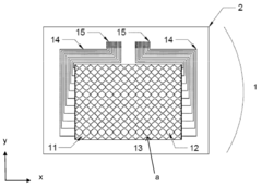
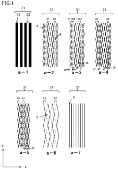
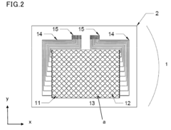
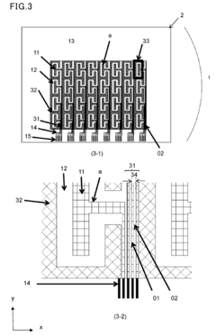
01 Metal mesh structure for enhanced conductivity
Metal mesh structures can be designed with specific patterns and dimensions to enhance electrical conductivity. These structures typically consist of interconnected metal lines forming a grid pattern, which provides conductive pathways while maintaining transparency or other desired properties. The geometry, thickness, and spacing of the metal lines can be optimized to achieve the desired conductivity while balancing other performance requirements.- Metal mesh structure for enhanced conductivity: Metal mesh structures can be designed with specific patterns and dimensions to enhance electrical conductivity. These structures typically consist of interconnected metal lines forming a grid or mesh pattern. The conductivity can be optimized by adjusting the thickness, width, and spacing of the metal lines. Such mesh structures provide a balance between transparency and conductivity, making them suitable for various electronic applications.
- Material composition for conductive metal meshes: The choice of materials significantly affects the conductivity of metal meshes. Various metals and alloys such as silver, copper, aluminum, and their combinations are used to create highly conductive meshes. Additionally, composite materials incorporating nanomaterials or conductive polymers can enhance the electrical properties while maintaining flexibility. Surface treatments and coatings can further improve conductivity by preventing oxidation and reducing contact resistance.
- Fabrication techniques for conductive metal meshes: Various manufacturing methods are employed to create metal meshes with optimal conductivity. These include photolithography, electroplating, etching, printing techniques, and laser patterning. Each method offers different advantages in terms of precision, scalability, and cost-effectiveness. Advanced fabrication techniques can produce meshes with nanoscale features that enhance conductivity while maintaining high transparency, which is crucial for applications in displays and touch sensors.
- Applications of conductive metal meshes in electronic devices: Conductive metal meshes are widely used in various electronic applications including touchscreens, displays, electromagnetic interference (EMI) shielding, and flexible electronics. The mesh structure allows for a combination of electrical conductivity and optical transparency, making these materials particularly valuable for display technologies. In addition, metal meshes can be integrated into wearable devices, solar cells, and sensors where both flexibility and conductivity are required.
- Environmental factors affecting metal mesh conductivity: The conductivity of metal meshes can be significantly affected by environmental factors such as temperature, humidity, and exposure to corrosive substances. Protective coatings and encapsulation techniques are often employed to maintain conductivity under varying conditions. Additionally, mechanical stress and deformation can impact the electrical properties of metal meshes, particularly in flexible or stretchable applications. Design considerations must account for these factors to ensure consistent performance over time.
02 Material composition for conductive metal meshes
The choice of materials significantly impacts the conductivity of metal meshes. Various metals and alloys can be used, including silver, copper, aluminum, and gold, each offering different conductivity levels and other properties. Some designs incorporate composite materials or multi-layered structures to enhance conductivity while providing additional benefits such as corrosion resistance or improved adhesion to substrates.Expand Specific Solutions03 Manufacturing techniques for conductive metal meshes
Various manufacturing methods can be employed to create metal meshes with optimal conductivity. These include photolithography, electroplating, etching, printing techniques, and deposition methods. Each manufacturing approach affects the final conductivity through factors such as edge definition, material purity, and structural integrity. Advanced manufacturing techniques can produce finer mesh patterns with improved conductivity characteristics.Expand Specific Solutions04 Surface treatments and coatings for conductivity enhancement
Surface treatments and coatings can significantly improve the conductivity of metal meshes. These treatments may include cleaning processes to remove contaminants, application of anti-oxidation layers to prevent degradation, or addition of conductive coatings to enhance performance. Some approaches involve post-processing techniques such as annealing or chemical treatments to optimize the conductive properties of the metal mesh structure.Expand Specific Solutions05 Applications of conductive metal meshes
Conductive metal meshes find applications in various fields where electrical conductivity combined with other properties is required. These include transparent conductive electrodes for touch screens and displays, electromagnetic interference (EMI) shielding, heating elements, sensors, and antennas. The specific conductivity requirements vary by application, influencing the design parameters and materials selected for the metal mesh structure.Expand Specific Solutions
Key Industry Players in Metal Mesh Development
The metal mesh conductivity market in electronic applications is currently in a growth phase, characterized by increasing demand for transparent conductive materials in displays, touch panels, and flexible electronics. The global market size is expanding rapidly, driven by the proliferation of smartphones, tablets, and emerging applications in automotive displays. Technologically, the field shows varying maturity levels, with established players like Samsung Electronics, BOE Technology, and Taiwan Semiconductor Manufacturing leading innovation through advanced manufacturing processes. Companies such as Sumitomo Electric, FUJIFILM, and NXP Semiconductors are developing specialized applications, while research institutions like Beijing University of Technology and McGill University contribute fundamental advancements. The competitive landscape features both large electronics manufacturers and specialized materials companies like Wacker Chemie and ROHM, indicating a diversifying ecosystem as the technology finds applications across multiple industries.
BOE Technology Group Co., Ltd.
Technical Solution: BOE has developed advanced metal mesh conductivity solutions for touch panels and displays, focusing on ultra-fine metal mesh structures with line widths below 5μm. Their proprietary patterning technology creates invisible conductive grids that maintain over 90% optical transparency while achieving sheet resistance below 10 ohms/square. BOE implements a multi-layer metal mesh architecture that combines silver and copper nanowires to optimize both conductivity and durability. Their manufacturing process includes specialized anti-oxidation coatings that extend the operational lifespan of metal mesh components by up to 40% compared to conventional implementations. For flexible display applications, BOE has pioneered stretchable metal mesh designs that maintain conductivity even under repeated bending cycles, with less than 5% resistance change after 100,000 flexing operations.
Strengths: Superior optical transparency while maintaining excellent conductivity; advanced manufacturing capabilities for ultra-fine metal mesh structures; proven durability in flexible applications. Weaknesses: Higher production costs compared to ITO alternatives; potential for visible moiré patterns in certain display configurations; requires specialized manufacturing equipment.
Samsung Electronics Co., Ltd.
Technical Solution: Samsung has pioneered hybrid metal mesh technology that combines nanoscale silver mesh with graphene interlayers to achieve exceptional conductivity in flexible electronic applications. Their approach features a proprietary mesh geometry with hexagonal patterns that optimize conductivity while minimizing optical interference. Samsung's metal mesh solutions achieve sheet resistance as low as 5 ohms/square while maintaining transparency above 92%. For foldable displays, Samsung has developed a specialized metal mesh architecture that can withstand over 200,000 folding cycles with less than 8% change in resistance. Their manufacturing process incorporates roll-to-roll techniques that enable cost-effective production at scale. Samsung has also developed self-healing metal mesh structures that can recover from minor damage through localized electrical current application, extending component lifespan in consumer electronics. Their latest research focuses on temperature-stable metal mesh conductors that maintain consistent performance from -40°C to +85°C.
Strengths: Industry-leading durability for foldable applications; excellent balance of transparency and conductivity; advanced self-healing capabilities for extended product life. Weaknesses: Complex manufacturing process increases production costs; proprietary technology creates vendor lock-in; requires specialized testing equipment to verify performance specifications.
Critical Patents and Innovations in Metal Mesh Technology
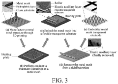
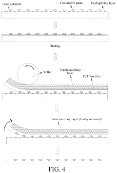
Manufacturing method of embedded metal mesh flexible transparent conductive film and application thereof
PatentActiveUS11551833B2
Innovation
- Combining electric-field-driven jet deposition micro-nano 3D printing with roll-to-plane thermal imprinting to create embedded metal mesh flexible transparent electrodes, allowing for low-cost, high-throughput production with high-temperature metal mesh materials and achieving low sheet resistance and high light transmittance.
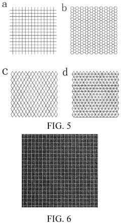
Light-transmitting conductive material
PatentInactiveUS20180024689A1
Innovation
- An optically transparent conductive material featuring a pattern of metal thin wires with a combination of main and satellite cells, where the number of cells sharing a side or vertex with the main cell is greater than with the satellite cell, and the longest distance between points on the main cell is longer than its width, reducing moire occurrence and optimizing conductivity and optical transparency.
Material Science Advancements for Metal Mesh Applications
Recent advancements in material science have significantly transformed the landscape of metal mesh applications in electronics. The evolution of nanomaterials and composite structures has enabled the development of metal meshes with unprecedented conductivity-to-transparency ratios. Silver nanowire networks, in particular, have emerged as frontrunners due to their exceptional electrical properties while maintaining optical transparency, crucial for touchscreen and display technologies.
Copper-based metal meshes have undergone substantial improvements through innovative surface treatments and alloying techniques. These advancements have addressed previous limitations related to oxidation and corrosion resistance, extending the operational lifespan of electronic components in diverse environmental conditions. The introduction of anti-corrosion coatings with nanometer thickness preserves conductivity while enhancing durability.
Hybrid metal mesh structures incorporating graphene and carbon nanotubes represent a paradigm shift in conductive material design. These composites leverage the mechanical flexibility of carbon allotropes while maintaining the superior conductivity of metallic elements. Research indicates that such hybrid structures can achieve conductivity values approaching 90% of bulk metals while remaining flexible enough for integration into wearable electronics.
Manufacturing processes have evolved concurrently with material innovations. Roll-to-roll fabrication techniques now enable the mass production of metal meshes with feature sizes below 5 micrometers, dramatically reducing production costs while maintaining precise geometric control. Laser-assisted direct writing methods have further expanded design possibilities, allowing for customized mesh patterns optimized for specific electronic applications.
Self-healing metal mesh technologies represent perhaps the most revolutionary advancement in recent years. These materials incorporate microencapsulated conductive elements that can repair minor damages autonomously, addressing one of the most persistent reliability challenges in flexible electronics. Early implementations have demonstrated the ability to restore up to 85% of original conductivity after mechanical damage.
Environmentally sustainable approaches to metal mesh production have gained significant traction, with particular focus on reducing dependence on rare earth elements. Aluminum-based meshes enhanced with carbon nanomaterials offer a more abundant alternative to indium-based transparent conductors, potentially resolving supply chain vulnerabilities while maintaining performance specifications required for modern electronic devices.
Environmental Impact and Sustainability Considerations
The environmental impact of metal mesh conductivity technologies in electronic applications represents a critical consideration in today's sustainability-focused industrial landscape. Metal mesh manufacturing processes typically involve resource-intensive extraction of raw materials, including copper, silver, aluminum, and gold. These extraction activities contribute significantly to habitat destruction, soil degradation, and water pollution in mining regions. Additionally, the chemical etching and plating processes commonly employed in metal mesh production generate hazardous waste containing heavy metals and acidic solutions that require specialized disposal protocols.
Energy consumption presents another substantial environmental concern. The high-temperature annealing and precision manufacturing techniques necessary for creating high-conductivity metal meshes demand considerable energy inputs, contributing to carbon emissions when powered by non-renewable energy sources. This energy footprint extends throughout the product lifecycle, from raw material extraction to manufacturing and eventual disposal.
The recyclability of metal mesh components offers a promising avenue for sustainability improvement. Unlike many electronic components, metal meshes can be effectively recovered and recycled, particularly those composed of precious metals like gold and silver. Implementing closed-loop recycling systems could significantly reduce the environmental burden associated with virgin material extraction while conserving valuable resources. Several leading manufacturers have already established take-back programs specifically targeting the recovery of metal components from electronic waste.
Emerging sustainable alternatives are gaining traction in the industry. Bio-based conductive materials derived from cellulose and other renewable resources show promise as potential replacements for traditional metal meshes in certain applications. Additionally, advancements in manufacturing techniques, such as additive printing methods, can substantially reduce material waste compared to traditional subtractive processes like etching.
Regulatory frameworks worldwide are increasingly addressing the environmental impacts of electronic components. The European Union's Restriction of Hazardous Substances (RoHS) directive and similar regulations in other regions have prompted manufacturers to develop metal mesh technologies with reduced environmental hazards. Furthermore, extended producer responsibility policies are shifting the burden of end-of-life management onto manufacturers, incentivizing more sustainable design approaches.
Looking forward, the industry faces both challenges and opportunities in balancing performance requirements with environmental considerations. Developing metal mesh technologies that maintain high conductivity while minimizing environmental impact will require continued innovation in materials science, manufacturing processes, and recycling technologies. Companies that successfully navigate these challenges stand to gain competitive advantage in an increasingly environmentally conscious marketplace.
Unlock deeper insights with Patsnap Eureka Quick Research — get a full tech report to explore trends and direct your research. Try now!
Generate Your Research Report Instantly with AI Agent
Supercharge your innovation with Patsnap Eureka AI Agent Platform!