Patents in the Metal Mesh Manufacturing Space
SEP 25, 20259 MIN READ
Generate Your Research Report Instantly with AI Agent
Patsnap Eureka helps you evaluate technical feasibility & market potential.
Metal Mesh Technology Evolution and Objectives
Metal mesh technology has evolved significantly over the past decades, transforming from simple wire mesh structures to sophisticated transparent conductive films that serve as critical components in modern electronic devices. The journey began in the 1990s with basic metal grid patterns primarily used for electromagnetic interference (EMI) shielding applications. By the early 2000s, advancements in microfabrication techniques enabled the production of finer metal meshes with improved optical transparency and electrical conductivity.
The pivotal breakthrough came around 2010 when metal mesh technology emerged as a viable alternative to indium tin oxide (ITO) for touch panels and displays. This shift was driven by ITO's inherent limitations including brittleness, limited supply of indium, and relatively high sheet resistance at larger dimensions. Metal mesh offered superior flexibility, lower resistance, and potentially lower manufacturing costs.
From 2010 to 2015, the patent landscape in metal mesh manufacturing expanded dramatically, with innovations focusing on novel fabrication methods such as nanoimprint lithography, gravure printing, and roll-to-roll processing. These patents aimed to address key challenges in mass production, including pattern uniformity, adhesion to substrates, and cost-effective scaling.
Between 2015 and 2020, patent activities shifted toward enhancing mesh performance characteristics, with particular emphasis on reducing visibility, improving durability, and developing self-healing properties. Companies began patenting specialized metal alloys and composite structures designed specifically for touch sensor applications.
The current technological objectives in metal mesh manufacturing center around several key areas. First is the development of ultra-fine mesh structures with line widths below 1 micron to achieve optical transparency exceeding 90% while maintaining sheet resistance below 10 ohms per square. Second is the advancement of manufacturing processes that reduce production costs and environmental impact while increasing yield rates.
Another critical objective is the integration of additional functionalities into metal mesh structures, such as antimicrobial properties, self-cleaning capabilities, and enhanced durability against repeated flexing and environmental factors. Patents in this area reflect growing interest in multi-functional materials that can serve multiple purposes in a single component.
Looking forward, the technology roadmap for metal mesh manufacturing is increasingly focused on sustainability and compatibility with flexible, foldable, and stretchable electronics. Recent patent filings indicate significant research into biodegradable substrates, environmentally friendly processing methods, and designs optimized for circular economy principles.
Market Analysis for Metal Mesh Applications
The metal mesh market has experienced significant growth over the past decade, driven primarily by the expanding touchscreen device industry. The global metal mesh market was valued at approximately 4.5 billion USD in 2022 and is projected to reach 7.8 billion USD by 2028, representing a compound annual growth rate of 9.6%. This growth trajectory is supported by increasing demand across multiple sectors including consumer electronics, automotive displays, and industrial applications.
Consumer electronics remains the dominant application segment, accounting for over 60% of the total market share. Within this segment, smartphones and tablets constitute the largest sub-segment, followed by laptops and all-in-one computers. The automotive sector represents the fastest-growing application area, with a projected growth rate of 12.3% annually through 2028, as vehicle manufacturers increasingly incorporate touch-enabled displays in their designs.
Geographically, Asia-Pacific leads the market with approximately 45% share, attributed to the concentration of electronics manufacturing facilities in countries like China, Taiwan, South Korea, and Japan. North America and Europe follow with 25% and 20% market shares respectively, with particular strength in high-end applications and research activities.
The demand for metal mesh technology is being driven by several key factors. First, the superior optical performance compared to alternative technologies like ITO (Indium Tin Oxide) provides better transparency and lower haze. Second, metal mesh offers excellent conductivity while maintaining flexibility, making it ideal for emerging form factors such as foldable displays. Third, the technology's scalability to larger screen sizes addresses the growing demand for larger touch displays in commercial and industrial settings.
Market analysis indicates that silver-based metal mesh currently dominates with approximately 70% market share, though copper-based solutions are gaining traction due to cost advantages. The manufacturing process landscape shows photolithography maintaining leadership position with 45% market share, while emerging techniques such as gravure printing and nanoimprint lithography are showing promising growth rates of 15% and 18% respectively.
Key challenges affecting market adoption include production costs, which remain higher than some competing technologies, and integration complexities when implementing metal mesh in certain device architectures. However, recent patent activities suggest significant innovation in manufacturing processes that may address these barriers in the near term.
Technical Challenges in Metal Mesh Manufacturing
Metal mesh manufacturing faces several significant technical challenges that impede production efficiency, quality consistency, and cost-effectiveness. The primary challenge lies in achieving uniform mesh structures with precise dimensions at nanometer or micrometer scales. Current manufacturing processes struggle to maintain consistent wire diameter, spacing, and junction integrity across large production areas, resulting in performance variations in the final products.
Material selection presents another substantial hurdle. While copper remains the industry standard due to its excellent conductivity, it is prone to oxidation and corrosion, significantly reducing product lifespan. Alternative materials like silver offer superior conductivity but at prohibitively higher costs, while aluminum and various alloys present their own processing difficulties related to malleability and durability.
The junction formation between intersecting wires represents a critical technical bottleneck. These junctions must maintain both structural integrity and electrical conductivity while minimizing resistance. Current welding and bonding techniques often create weak points in the mesh structure or introduce excessive resistance that compromises overall performance.
Surface treatment technologies face limitations in achieving optimal transparency while maintaining conductivity. The trade-off between these properties remains challenging, particularly for applications in display technologies where both characteristics are equally important. Existing coating methods often fail to provide uniform protection against environmental factors without degrading electrical performance.
Manufacturing scalability constitutes a significant challenge, particularly in transitioning from laboratory-scale production to industrial-scale manufacturing. Roll-to-roll processing, while promising for high-volume production, introduces tension control issues that can distort mesh geometry. Additionally, inspection and quality control systems struggle to detect microscopic defects at production speeds.
Environmental considerations add another layer of complexity. Traditional metal mesh manufacturing processes often involve hazardous chemicals for etching and cleaning. Developing environmentally friendly alternatives that maintain production efficiency and product quality remains an ongoing challenge for the industry.
Integration challenges also exist when incorporating metal mesh into final products. Adhesion to substrates, particularly flexible ones, presents difficulties in maintaining electrical continuity during bending and folding operations. Furthermore, connection technologies between the mesh and external circuitry often create reliability issues at these transition points.
Current Metal Mesh Manufacturing Methods
01 Metal mesh for electronic devices
Metal mesh structures are used in electronic devices for various applications including touch screens, displays, and sensors. These meshes provide electrical conductivity while maintaining optical transparency. The design often involves specific patterns and materials to optimize performance, including enhanced sensitivity, reduced interference, and improved durability for touch-based interactions.- Metal mesh for touch screen applications: Metal mesh structures are used in touch screen technologies to create transparent conductive patterns. These meshes provide electrical conductivity while maintaining optical transparency, making them ideal for touchscreens in various electronic devices. The mesh patterns can be designed with specific geometries to optimize both touch sensitivity and visual clarity. Advanced manufacturing techniques allow for creating ultra-fine metal mesh patterns that are nearly invisible to the naked eye.
- Metal mesh for electromagnetic shielding: Metal mesh structures are utilized for electromagnetic interference (EMI) shielding in electronic devices. These meshes can block or attenuate electromagnetic radiation while allowing for ventilation and heat dissipation. The mesh design parameters such as wire diameter, opening size, and material composition can be optimized for specific frequency ranges of electromagnetic radiation. This application is particularly important in sensitive electronic equipment and communication devices.
- Manufacturing processes for metal mesh structures: Various manufacturing techniques are employed to produce metal mesh structures with precise specifications. These include photolithography, etching, electroforming, and advanced printing methods. The manufacturing processes can control critical parameters such as mesh thickness, pattern geometry, and material composition. Innovations in production methods focus on improving yield rates, reducing costs, and enabling mass production of high-precision metal mesh components.
- Metal mesh for filtration and separation applications: Metal mesh structures are designed for filtration and separation processes across various industries. The mesh specifications can be tailored for specific particle sizes, flow rates, and operating conditions. These meshes offer advantages such as high strength, temperature resistance, and chemical compatibility compared to non-metallic alternatives. Applications include industrial filtration, food processing, pharmaceutical manufacturing, and environmental protection systems.
- Metal mesh for energy applications: Metal mesh structures are utilized in various energy-related applications including batteries, fuel cells, and solar technologies. The mesh design provides electrical conductivity while maintaining structural integrity and allowing for material or energy flow. These meshes can serve as current collectors, electrodes, or structural supports in energy storage and generation devices. Advanced coatings and surface treatments can enhance the performance characteristics of metal meshes in specific energy applications.
02 Manufacturing processes for metal mesh
Various manufacturing techniques are employed to produce metal mesh structures with precise specifications. These processes include etching, electroforming, laser cutting, and additive manufacturing methods. The manufacturing approach affects the mesh properties such as wire diameter, opening size, uniformity, and overall structural integrity, which are critical for the intended application performance.Expand Specific Solutions03 Metal mesh for filtration and separation
Metal meshes are utilized in filtration and separation systems across various industries. These meshes feature specific pore sizes and configurations designed to separate particles, filter fluids, or screen materials. The mesh design considers factors such as flow rate, pressure drop, clogging resistance, and mechanical strength to ensure efficient separation while maintaining structural integrity under operating conditions.Expand Specific Solutions04 Protective and structural metal mesh applications
Metal meshes serve as protective barriers and structural components in various applications. These include safety guards, reinforcement elements, architectural features, and enclosures. The mesh design balances strength, weight, visibility, and aesthetic considerations while providing protection against physical intrusion, environmental factors, or containing materials within a defined space.Expand Specific Solutions05 Specialized coatings and treatments for metal mesh
Metal meshes often undergo specialized surface treatments and coatings to enhance their properties. These treatments can improve corrosion resistance, wear resistance, electrical conductivity, or add functionality such as hydrophobic or antimicrobial properties. The coating processes are tailored to the specific mesh structure and intended application environment to optimize performance and extend service life.Expand Specific Solutions
Key Industry Players and Patent Holders
The metal mesh manufacturing space is currently in a growth phase, characterized by increasing market adoption across electronics, automotive, and industrial sectors. The market is projected to reach significant scale due to rising demand for touch panels, displays, and advanced electronic components. Technologically, the field shows varying maturity levels, with established players like Texas Instruments, Taiwan Semiconductor, and BOE Technology Group demonstrating advanced capabilities in metal mesh fabrication. Companies such as 3M Innovative Properties and AT&S Austria are developing specialized applications, while newer entrants like Shenzhen Zhi Ling Wei Ye Technology are focusing on touch panel implementations. The competitive landscape is diversifying as both semiconductor giants and specialized manufacturers compete to establish intellectual property positions in this high-potential manufacturing domain.
Taiwan Semiconductor Manufacturing Co., Ltd.
Technical Solution: TSMC has developed sophisticated metal mesh manufacturing technologies leveraging their semiconductor expertise. Their approach utilizes advanced lithography and etching processes adapted from semiconductor manufacturing to create ultra-precise metal mesh structures with line widths as small as 1 micron. TSMC's patented technology incorporates multi-layer metal stacking techniques that enhance conductivity while maintaining optical transparency above 85%. The company employs specialized deposition methods that ensure uniform metal distribution and excellent adhesion to various substrate materials. Their manufacturing process includes proprietary cleaning and surface preparation steps that significantly reduce defect rates. TSMC has also patented unique metal alloy formulations specifically designed to optimize the performance-to-cost ratio in touch panel applications. Their technology enables the creation of complex mesh patterns with variable density across a single substrate, allowing for optimized performance in different functional areas of the same device.
Strengths: Exceptional precision and uniformity leveraging semiconductor manufacturing expertise; advanced multi-layer capabilities; excellent scalability for high-volume production. Weaknesses: Higher production costs compared to traditional methods; primarily focused on rigid substrate applications; requires specialized equipment that limits manufacturing flexibility.
BOE Technology Group Co., Ltd.
Technical Solution: BOE has pioneered metal mesh manufacturing technologies specifically optimized for large-format display applications. Their patented approach employs a unique combination of nano-imprint lithography and electroplating processes to create highly uniform metal mesh structures across large surface areas. BOE's technology achieves line widths of approximately 2-3 microns with spacing optimized to minimize moiré patterns when overlaid with display pixels. The company has developed proprietary metal alloy formulations that enhance conductivity while maintaining excellent adhesion to various substrate materials. Their manufacturing process incorporates in-line quality control systems using machine vision to detect and address defects in real-time. BOE has also patented specialized encapsulation techniques that protect the metal mesh structures from environmental degradation and oxidation, significantly extending the operational lifetime of their touch panels and display components.
Strengths: Exceptional expertise in large-format applications; highly automated production processes enabling consistent quality; strong integration capabilities with display manufacturing. Weaknesses: Technology primarily optimized for flat panel applications with less focus on flexible substrates; higher capital investment requirements for production facilities; somewhat limited in ultra-fine mesh applications below 2 micron linewidths.
Critical Patent Analysis and IP Landscape
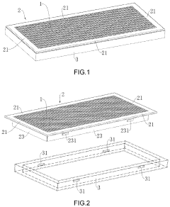
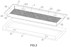
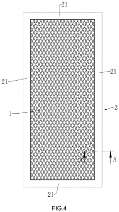
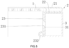
Low-cost, high-strength and easy-to-assemble metal mesh plate structure
PatentActiveUS20230160259A1
Innovation
- A low-cost, high-strength metal mesh plate structure featuring an outer frame with clamping parts and a reinforcing folding part that enhances rigidity, along with a reinforcing frame body for additional support, eliminating visible screws and allowing for different colors to meet aesthetic requirements, while maintaining simplicity and ease of assembly.
Porous substrates for implantation
PatentInactiveEP2112934A2
Innovation
- A porous substrate is created using a three-dimensional modeling process to form an open-cell pore network, allowing for varying pore volume fractions and shapes to match physiological loading conditions, reducing material usage and enhancing bone integration by mimicking natural bone structures.
Material Science Advancements for Metal Mesh
Recent advancements in material science have significantly transformed the metal mesh manufacturing landscape. The evolution of nanomaterials has enabled the production of ultra-thin metal meshes with enhanced conductivity and flexibility, critical for next-generation touch sensors and electromagnetic shielding applications. These innovations have reduced mesh thickness to below 5 microns while maintaining structural integrity and electrical performance.
Composite metal alloys represent another breakthrough area, where combinations of silver, copper, aluminum, and nickel create meshes with optimized properties for specific applications. These alloys demonstrate superior corrosion resistance and thermal stability compared to traditional single-metal meshes, extending product lifespan in harsh environments.
Surface treatment technologies have evolved to address oxidation and degradation challenges. Advanced anti-corrosion coatings using atomic layer deposition techniques provide nanometer-thick protective layers without compromising optical transparency or electrical conductivity. Self-healing coating systems incorporating microencapsulated healing agents have shown promising results in laboratory settings, potentially extending mesh lifespan by 40-60%.
Sustainable manufacturing processes are gaining prominence with the development of eco-friendly etching solutions that replace traditional acid-based processes. Water-based and biodegradable etching compounds reduce environmental impact while maintaining precision in pattern formation. Additionally, recycling technologies specifically designed for metal mesh waste recovery have achieved material reclamation rates exceeding 85%.
Biomimetic approaches have inspired novel mesh designs that emulate natural structures for enhanced performance. Spider-web-inspired geometries demonstrate superior strength-to-weight ratios, while lotus-leaf-inspired surface treatments create self-cleaning properties that maintain optical clarity and conductivity in challenging environments.
Computational materials science has accelerated development through predictive modeling of material behaviors under various conditions. Machine learning algorithms now optimize alloy compositions and manufacturing parameters, reducing development cycles from years to months while identifying previously unexplored material combinations with superior performance characteristics.
Environmental Impact and Sustainability Considerations
Metal mesh manufacturing processes have traditionally been associated with significant environmental impacts, including high energy consumption, greenhouse gas emissions, and waste generation. Recent patent innovations in this space increasingly focus on addressing these sustainability challenges. Advanced manufacturing techniques such as precision laser cutting and additive manufacturing have demonstrated potential to reduce material waste by up to 30% compared to conventional methods. These technologies enable more efficient material utilization through optimized nesting patterns and reduced trim scrap.
Water usage represents another critical environmental concern in metal mesh production. Patents filed in the last five years show a growing trend toward closed-loop water systems that can recycle up to 95% of process water. These innovations incorporate advanced filtration technologies to remove contaminants while maintaining water quality suitable for continued manufacturing operations, significantly reducing freshwater consumption and wastewater discharge.
Energy efficiency improvements feature prominently in recent patent filings, with innovations targeting reduced energy consumption during high-temperature processes. Novel heating methods utilizing induction technology and precision temperature control systems have demonstrated energy savings of 15-25% compared to traditional manufacturing approaches. Additionally, patents covering recovery systems that capture and repurpose waste heat from production processes further enhance overall energy efficiency.
Chemical usage in metal mesh manufacturing presents both environmental and health concerns. Patent activity shows increasing focus on developing less toxic alternatives to traditional chemical treatments and coatings. Bio-based solutions and water-based formulations are emerging as viable replacements for solvent-based systems, reducing volatile organic compound (VOC) emissions and improving workplace safety conditions.
End-of-life considerations are gaining prominence in metal mesh patents, with innovations addressing recyclability and material recovery. Advanced alloy designs maintain performance characteristics while facilitating easier separation and recycling. Some patents describe manufacturing processes specifically optimized to produce metal mesh products that can be completely reprocessed at end-of-life, supporting circular economy principles.
Carbon footprint reduction strategies appear in patents combining multiple sustainability approaches, including renewable energy integration with manufacturing processes. Several innovations describe systems that can dynamically adjust production parameters based on available renewable energy, potentially reducing carbon emissions by 40-60% compared to conventional manufacturing methods relying solely on grid electricity.
Unlock deeper insights with Patsnap Eureka Quick Research — get a full tech report to explore trends and direct your research. Try now!
Generate Your Research Report Instantly with AI Agent
Supercharge your innovation with Patsnap Eureka AI Agent Platform!