Patent Overview: Metal Mesh in Electronics and Communication
SEP 25, 20259 MIN READ
Generate Your Research Report Instantly with AI Agent
Patsnap Eureka helps you evaluate technical feasibility & market potential.
Metal Mesh Technology Evolution and Objectives
Metal mesh technology has evolved significantly over the past decades, transforming from simple conductive grids to sophisticated nanoscale structures with diverse applications in electronics and communication. The journey began in the early 2000s with basic metal mesh designs primarily used for electromagnetic interference (EMI) shielding. These early implementations featured relatively large grid patterns with limited transparency and flexibility, constraining their application potential.
By the mid-2000s, advancements in manufacturing techniques, particularly photolithography and etching processes, enabled the production of finer mesh structures with improved optical transparency while maintaining electrical conductivity. This marked a pivotal shift in the technology's trajectory, opening doors to applications in transparent electrodes for touch screens and displays.
The 2010s witnessed a revolutionary phase in metal mesh development with the introduction of nanoimprint lithography and roll-to-roll manufacturing processes. These innovations dramatically reduced production costs while enhancing performance metrics such as sheet resistance, optical clarity, and mechanical durability. Concurrently, the integration of metal mesh technology with flexible substrates expanded its application scope to wearable electronics and curved displays.
Recent years have seen the emergence of hybrid metal mesh structures incorporating nanomaterials like graphene and carbon nanotubes, creating composite systems with superior performance characteristics. These hybrid structures address previous limitations in conductivity-transparency trade-offs and mechanical flexibility, pushing the boundaries of what's achievable with transparent conductive materials.
The primary technological objectives for metal mesh development focus on several key areas. First, enhancing the optical transparency while maintaining or improving electrical conductivity remains a central challenge, particularly for high-resolution display applications. Second, improving mechanical durability and flexibility is crucial for emerging applications in foldable devices and wearable technology. Third, developing cost-effective, scalable manufacturing processes is essential for widespread commercial adoption.
Additionally, researchers aim to optimize metal mesh designs for specific wavelength interactions, particularly in the context of 5G and future communication technologies where millimeter-wave transmission and reception are critical. The integration of metal mesh with other functional materials to create multifunctional surfaces represents another important objective, potentially enabling surfaces that simultaneously serve as antennas, touch sensors, and display components.
The evolution trajectory suggests that metal mesh technology will continue to advance toward nanoscale precision, multifunctionality, and seamless integration with various electronic systems, positioning it as a cornerstone technology for next-generation electronics and communication devices.
Market Analysis for Metal Mesh Applications
The metal mesh market in electronics and communication has experienced significant growth over the past decade, driven primarily by the expanding touchscreen device industry. The global metal mesh market was valued at approximately $187 million in 2020 and is projected to reach $328 million by 2026, growing at a CAGR of 9.8% during the forecast period. This growth trajectory is supported by increasing demand for smartphones, tablets, laptops, and other consumer electronic devices that incorporate touchscreen technology.
Consumer electronics represents the largest application segment for metal mesh technology, accounting for nearly 65% of the total market share. Within this segment, smartphones dominate with approximately 40% market share, followed by tablets and laptops. The automotive sector is emerging as the fastest-growing application area, with a projected CAGR of 12.3% through 2026, as vehicle manufacturers increasingly incorporate touch displays in their infotainment systems and control panels.
Geographically, Asia-Pacific leads the metal mesh market with approximately 58% of global market share, primarily due to the concentration of electronics manufacturing facilities in countries like China, South Korea, Japan, and Taiwan. North America and Europe follow with 22% and 15% market shares respectively, with growth in these regions driven by adoption in premium electronic devices and automotive applications.
The market is witnessing several notable trends that are shaping its development. First, there is increasing preference for metal mesh over competing technologies like ITO (Indium Tin Oxide) due to its superior conductivity, flexibility, and cost-effectiveness. Second, the growing demand for larger touchscreen displays in various applications is favoring metal mesh technology due to its scalability advantages. Third, the emergence of foldable and flexible display technologies is creating new opportunities for metal mesh applications.
Key market challenges include competition from alternative technologies such as silver nanowires and carbon nanotubes, as well as technical challenges related to optical performance and manufacturing complexity. However, ongoing innovations in manufacturing processes and material science are gradually addressing these limitations.
The market forecast indicates continued strong growth, particularly in emerging applications such as transparent antennas for 5G devices, EMI shielding solutions, and transparent heaters for automotive and aerospace applications. These diversified applications are expected to reduce market volatility and create sustainable growth opportunities for metal mesh technology providers in the coming years.
Technical Challenges and Global Development Status
Metal mesh technology in electronics and communication faces several significant technical challenges despite its promising applications. The primary obstacle remains achieving the optimal balance between optical transparency and electrical conductivity. Current manufacturing processes struggle to produce meshes with line widths below 1 μm while maintaining high conductivity, creating a fundamental trade-off that limits performance in display applications.
Durability presents another major challenge, as metal meshes are susceptible to oxidation and mechanical damage, particularly in flexible or wearable devices. The industry continues to search for effective protective coatings that don't compromise electrical or optical properties. Additionally, manufacturing scalability remains problematic, with high-precision techniques like photolithography proving costly for mass production.
Globally, metal mesh technology development shows distinct regional characteristics. North America leads in research innovation, with companies like 3M and universities such as MIT pioneering novel fabrication methods. Asia, particularly South Korea, Japan, and China, dominates commercial production, with companies like LG Display and Shenzhen O-Film Tech holding significant market share and manufacturing capacity.
Europe contributes substantially to materials science advancements, with research institutions in Germany and Finland developing hybrid materials that enhance metal mesh performance. The global patent landscape reveals concentrated ownership, with approximately 65% of metal mesh patents held by just 15 companies, indicating a relatively consolidated technology space.
Recent technological breakthroughs include self-healing metal mesh structures developed in Japan, which can repair minor damage through controlled electrical stimulation. Meanwhile, Chinese manufacturers have achieved notable success in cost reduction through roll-to-roll processing techniques, though quality consistency remains variable.
Standardization efforts remain fragmented across regions, creating interoperability challenges. The International Electrotechnical Commission has established working groups to address this gap, but comprehensive standards are still under development. This lack of standardization has slowed adoption in certain sectors, particularly automotive displays and medical devices.
Environmental concerns also shape development trajectories, with increasing regulatory pressure regarding the use of silver and other precious metals in mesh structures. Research into alternative materials like copper-nickel alloys and carbon-metal composites has accelerated in response, though these alternatives have yet to match the performance of traditional silver-based meshes.
Current Metal Mesh Implementation Approaches
01 Metal mesh for electronic devices
Metal mesh structures are used in electronic devices such as touch screens, displays, and sensors. These meshes provide electrical conductivity while maintaining optical transparency. The metal mesh patterns can be designed with specific geometries to optimize performance characteristics including conductivity, visibility, and durability. These structures are particularly valuable in touchscreen applications where both transparency and conductivity are required.- Metal mesh for touch screen applications: Metal mesh structures are used in touch screen technologies to create transparent conductive patterns. These meshes provide electrical conductivity while maintaining optical transparency, making them ideal for touchscreens in various electronic devices. The mesh design typically consists of fine metal lines arranged in specific patterns to optimize both conductivity and visibility. Advanced manufacturing techniques allow for creating ultra-thin metal lines that are nearly invisible to the naked eye while maintaining excellent touch sensitivity.
- Metal mesh for electromagnetic shielding: Metal mesh structures are utilized for electromagnetic interference (EMI) shielding in electronic devices. These meshes can block or attenuate electromagnetic radiation, protecting sensitive components from external interference or preventing signal leakage. The mesh design parameters, including aperture size, wire diameter, and material composition, can be optimized for specific frequency ranges. These shielding solutions are particularly important in high-frequency applications and densely packed electronic devices where signal integrity is crucial.
- Manufacturing methods for metal mesh structures: Various manufacturing techniques are employed to produce metal mesh structures with precise dimensions and properties. These methods include photolithography, etching, electroforming, and advanced printing techniques. The manufacturing processes can control critical parameters such as line width, spacing, thickness, and pattern geometry. Recent innovations focus on cost-effective mass production methods while maintaining high precision and quality, enabling the widespread application of metal mesh in consumer electronics and industrial applications.
- Metal mesh for filtration and separation applications: Metal mesh structures are designed for filtration and separation processes across various industries. These meshes feature precisely controlled pore sizes and distributions to effectively separate particles, molecules, or cells based on size. The durability of metal meshes makes them suitable for harsh environments involving high temperatures, pressures, or corrosive substances. Applications include industrial filtration, water treatment, food processing, and pharmaceutical manufacturing where precise separation capabilities and durability are required.
- Metal mesh for structural reinforcement: Metal mesh is used as reinforcement material in composite structures and construction applications. The mesh provides mechanical strength, impact resistance, and structural integrity while maintaining relatively low weight. Various mesh designs with different wire diameters, spacing, and patterns are employed depending on the specific load requirements and application environment. These reinforcement solutions are utilized in concrete structures, aerospace components, automotive parts, and other applications requiring enhanced mechanical properties.
02 Manufacturing methods for metal mesh
Various manufacturing techniques are employed to produce metal mesh structures with precise specifications. These methods include photolithography, etching, printing, and deposition processes. Advanced manufacturing approaches allow for the creation of ultra-fine mesh patterns with controlled dimensions and spacing. The manufacturing processes can be optimized to enhance production efficiency while maintaining high quality and consistency of the metal mesh structures.Expand Specific Solutions03 Metal mesh for filtration and separation
Metal mesh structures are utilized in filtration and separation applications across various industries. These meshes can be designed with specific pore sizes to filter particles, separate materials, or control fluid flow. The durability and corrosion resistance of certain metal alloys make these meshes suitable for harsh environments. Applications include industrial filtration, water treatment, food processing, and chemical separation processes.Expand Specific Solutions04 Metal mesh for electromagnetic shielding
Metal mesh structures provide effective electromagnetic interference (EMI) shielding in electronic devices and sensitive equipment. The mesh design allows for the blocking of electromagnetic radiation while maintaining other functional properties such as ventilation or visibility. The shielding effectiveness can be optimized by controlling the mesh density, material composition, and structural configuration. These solutions are implemented in various applications requiring protection from electromagnetic interference.Expand Specific Solutions05 Composite materials incorporating metal mesh
Metal mesh structures are integrated into composite materials to enhance mechanical properties and functionality. These composites combine the strength and conductivity of metal mesh with the properties of other materials such as polymers, ceramics, or other metals. The resulting composite materials offer improved characteristics including enhanced strength-to-weight ratio, thermal management, and electrical conductivity. Applications include aerospace components, construction materials, and specialized industrial products.Expand Specific Solutions
Industry Leaders and Competitive Landscape
The metal mesh technology in electronics and communication is currently in a growth phase, with an expanding market driven by increasing demand for advanced touchscreens, antennas, and EMI shielding solutions. The global market is estimated to reach significant scale as major players like Apple, Samsung, BOE Technology, and LG Electronics integrate metal mesh into their product ecosystems. Technologically, the field shows varying maturity levels across applications, with companies like SnapTrack and Microsoft focusing on wireless positioning technologies, while Asian manufacturers such as BOE, Shenzhen Zhi Ling Wei Ye, and Kunshan Innowave lead in display and communication implementations. Western technology giants including Apple, Intel, and IBM are advancing the integration capabilities through substantial R&D investments, pushing the boundaries of metal mesh applications in next-generation electronic devices.
Apple, Inc.
Technical Solution: Apple has developed advanced metal mesh technology for touchscreens and displays, utilizing a grid of ultra-thin metal traces that offer both conductivity and transparency. Their approach involves depositing metal layers (typically copper, silver, or aluminum) in precise patterns using photolithographic techniques, creating conductive pathways that remain virtually invisible to users. Apple's implementation includes multi-layer metal mesh structures with varying geometries to optimize touch sensitivity while minimizing optical interference. The company has integrated this technology into various products, including iPhones and iPads, where the metal mesh serves as transparent conductive electrodes that replace traditional indium tin oxide (ITO). Apple's patents show particular innovation in mesh pattern design that reduces moiré effects when overlaid with display pixels.
Strengths: Superior durability compared to ITO, allowing for flexible and foldable applications; better conductivity leading to improved touch response; cost-effective manufacturing at scale. Weaknesses: Potential for visible patterns under certain lighting conditions; more complex manufacturing process requiring precise deposition and etching techniques.
Samsung Electronics Co., Ltd.
Technical Solution: Samsung has pioneered metal mesh technology for flexible displays and communication devices, developing a proprietary fabrication process that creates nanoscale metal grid structures. Their approach utilizes silver nanowire networks embedded in polymer substrates, creating transparent conductive films with exceptional flexibility and durability. Samsung's metal mesh implementations feature hexagonal and diamond patterns that optimize conductivity while maintaining transparency above 90%. The company has integrated this technology into their foldable smartphones, where the metal mesh serves as both EMI shielding and touch sensors. Samsung's patents reveal innovations in self-healing metal mesh structures that can repair minor breaks in the conductive pathways through controlled electrical stimulation, extending the operational lifespan of flexible electronic devices.
Strengths: Excellent flexibility allowing for implementation in foldable devices; high conductivity-to-transparency ratio; resilience to repeated bending and folding. Weaknesses: Higher production costs compared to traditional rigid electronics; potential for oxidation of metal elements requiring additional protective layers.
Key Patents and Technical Breakthroughs
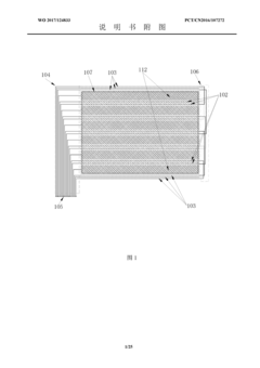
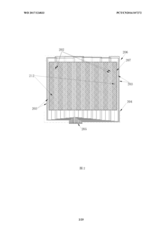
Metal mesh dual-touch sensor, touch module and electronic touch device
PatentWO2017124833A1
Innovation
- Integration of capacitive and electromagnetic touch functionality in a single metal mesh structure, allowing for dual-touch sensing capabilities while maintaining a simplified design.
- Ultrafine metal mesh design that is not directly distinguishable to the human eye, enabling placement directly on display screen surfaces without compromising visual quality.
- Cost-effective structural design with simplified manufacturing process, making touch technology more accessible for larger form factor devices.
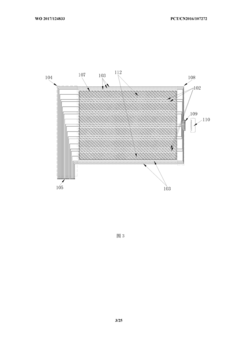
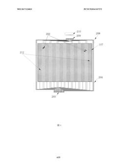
Metal mesh structure, touch display device and mobile terminal
PatentActiveUS11914830B2
Innovation
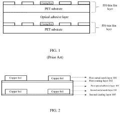
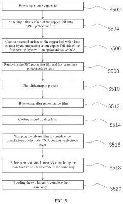
- A metal mesh structure for capacitive touch screens is developed, comprising multiple layers with specific thicknesses and materials, including coating layers on metal mesh layers, eliminating the need for a polymer substrate, which enhances conductivity, reduces surface resistance, and improves transmittance and thinness.
Material Science Advancements Supporting Metal Mesh
The evolution of metal mesh technology in electronics and communication has been significantly influenced by advancements in material science. Traditional metal mesh structures, primarily composed of copper, silver, or aluminum, have undergone substantial transformation through innovative material engineering approaches. These advancements have directly addressed key limitations such as conductivity, flexibility, and durability that previously hindered widespread adoption.
Nanomaterial integration represents one of the most impactful developments in metal mesh technology. The incorporation of carbon nanotubes (CNTs) and graphene into metal mesh structures has dramatically enhanced electrical conductivity while maintaining optical transparency. This hybrid approach has yielded mesh structures with sheet resistance values below 10 ohms/square while maintaining transparency above 90% - performance metrics previously unattainable with conventional materials.
Surface treatment technologies have also revolutionized metal mesh capabilities. Anti-corrosion coatings using specialized polymers and self-healing materials have extended the operational lifespan of metal mesh components in harsh environments. Additionally, hydrophobic and oleophobic surface treatments have improved touch sensitivity in display applications while reducing maintenance requirements.
Alloy development has emerged as another critical area of advancement. Novel metal alloys incorporating elements such as indium, molybdenum, and titanium have demonstrated superior performance characteristics compared to single-metal meshes. These alloys offer enhanced mechanical flexibility, reduced oxidation rates, and improved adhesion to substrate materials - critical factors for applications in flexible electronics.
Manufacturing process innovations have enabled the production of ultra-fine metal mesh structures with line widths below 2 micrometers. Techniques such as nanoimprint lithography, electrospinning, and directed self-assembly have facilitated the creation of mesh patterns with unprecedented precision and uniformity. These manufacturing advances have directly contributed to improved optical performance and reduced visibility of mesh patterns in display applications.
Substrate compatibility has been enhanced through the development of specialized interface materials that promote adhesion between metal meshes and various substrates including glass, polymers, and textiles. These interface materials not only improve mechanical stability but also mitigate issues related to thermal expansion mismatch, thereby extending device longevity and reliability in dynamic operating conditions.
Environmental Impact and Sustainability Considerations
The environmental impact of metal mesh technology in electronics and communication presents a complex sustainability challenge that requires careful consideration. The manufacturing processes for metal mesh components involve resource-intensive extraction of raw materials including silver, copper, aluminum, and other metals. These extraction activities contribute significantly to habitat destruction, soil degradation, and water pollution in mining regions. Additionally, the chemical etching and plating processes commonly used in metal mesh production generate hazardous waste containing heavy metals and acidic solutions that require specialized disposal protocols.
Energy consumption represents another critical environmental concern. The production of metal mesh components demands substantial energy inputs for processes such as vacuum deposition, photolithography, and thermal treatments. This energy footprint is particularly significant when considering the global scale of electronics manufacturing and the increasing integration of metal mesh technology across multiple device categories.
Recycling challenges further complicate the sustainability profile of metal mesh technology. The intricate integration of metal mesh with other electronic components creates significant barriers to end-of-life recovery and recycling. The ultrathin nature of many metal mesh structures makes separation from substrate materials technically difficult and economically challenging, resulting in substantial material loss during recycling processes.
Recent industry initiatives have begun addressing these environmental concerns through several promising approaches. Material innovation has led to the development of more environmentally benign manufacturing processes, including additive printing techniques that reduce waste generation compared to traditional subtractive methods. Some manufacturers have successfully implemented closed-loop water systems that minimize effluent discharge and reduce freshwater consumption in production facilities.
The potential for extended product lifecycles represents another sustainability opportunity. Metal mesh components generally offer superior durability compared to alternative technologies like ITO (Indium Tin Oxide), potentially extending device lifespans and reducing electronic waste generation. Furthermore, emerging design approaches emphasizing modular construction may facilitate easier component separation and material recovery at end-of-life.
Looking forward, the industry faces increasing regulatory pressure regarding environmental performance. Extended producer responsibility frameworks, restrictions on hazardous substances, and carbon pricing mechanisms are likely to shape future development trajectories for metal mesh technology. Companies investing in sustainable manufacturing processes and circular economy principles may gain competitive advantages as environmental considerations become increasingly central to technology evaluation and procurement decisions.
Unlock deeper insights with Patsnap Eureka Quick Research — get a full tech report to explore trends and direct your research. Try now!
Generate Your Research Report Instantly with AI Agent
Supercharge your innovation with Patsnap Eureka AI Agent Platform!