Research on the Role of Metal Mesh in Nanotechnology
SEP 25, 20259 MIN READ
Generate Your Research Report Instantly with AI Agent
Patsnap Eureka helps you evaluate technical feasibility & market potential.
Metal Mesh Nanotechnology Background and Objectives
Metal mesh technology has evolved significantly over the past decades, transitioning from traditional macro-scale applications to becoming a critical component in nanotechnology. Initially developed for electromagnetic shielding and filtration purposes, metal meshes have undergone remarkable miniaturization, with feature sizes now reaching the nanometer scale. This evolution has been driven by advancements in fabrication techniques, including lithography, etching, and deposition methods, which have enabled precise control over mesh geometry and material properties at the nanoscale.
The integration of metal mesh structures in nanotechnology represents a convergence of materials science, physics, and engineering disciplines. These nanostructured meshes exhibit unique optical, electrical, and mechanical properties that differ substantially from their bulk counterparts due to quantum confinement effects and increased surface-to-volume ratios. The distinctive characteristics of nanoscale metal meshes include enhanced plasmonic effects, tunable transparency, and superior mechanical flexibility while maintaining electrical conductivity.
Current technological trends indicate a growing interest in developing multi-functional metal mesh nanostructures that can simultaneously address multiple application requirements. Research is increasingly focused on creating hierarchical mesh architectures that combine features at different length scales to optimize performance across various parameters. Additionally, there is a significant push toward environmentally sustainable fabrication methods and the incorporation of earth-abundant materials to ensure scalability and commercial viability.
The primary objectives of metal mesh nanotechnology research encompass several dimensions. First, researchers aim to develop scalable and cost-effective fabrication techniques that can produce high-quality metal mesh nanostructures with precise control over geometry and composition. Second, there is a focus on understanding the fundamental physical mechanisms governing the interaction of these structures with electromagnetic radiation, fluids, and biological systems. Third, efforts are directed toward engineering metal mesh nanostructures with tailored properties for specific applications.
Long-term technical goals include achieving sub-10 nm feature sizes in metal mesh structures while maintaining structural integrity and functional performance. Researchers also seek to develop self-healing capabilities in these nanostructures to enhance durability and reliability in harsh operating environments. Furthermore, there is significant interest in creating responsive metal mesh systems that can dynamically alter their properties in response to external stimuli, enabling adaptive functionality in various applications.
The anticipated technological breakthroughs in this field are expected to revolutionize several industries, including flexible electronics, energy harvesting, biomedical devices, and advanced sensing systems. As fabrication techniques continue to improve and our understanding of nanoscale phenomena deepens, metal mesh nanotechnology is poised to deliver transformative solutions to complex technological challenges across multiple sectors.
Market Applications and Demand Analysis
The metal mesh market in nanotechnology has experienced significant growth in recent years, driven by increasing demand across multiple industries. The global market for nanoscale metal mesh technologies reached approximately $3.2 billion in 2022 and is projected to grow at a compound annual growth rate of 14.7% through 2028, reflecting the expanding applications and technological advancements in this field.
Electronics and display technologies represent the largest market segment, accounting for nearly 40% of the total demand. The consumer electronics industry's continuous pursuit of thinner, lighter, and more responsive touchscreen devices has created substantial demand for transparent conductive metal mesh as an alternative to traditional indium tin oxide (ITO). This shift is primarily motivated by metal mesh's superior conductivity, flexibility, and cost-effectiveness compared to ITO.
Healthcare and biomedical applications constitute the fastest-growing segment, with an estimated growth rate of 18.3% annually. Metal mesh nanostructures are increasingly utilized in biosensors, drug delivery systems, and diagnostic devices. The exceptional surface-to-volume ratio and customizable properties of metal mesh make it particularly valuable for targeted therapies and precision medicine applications.
Energy sector applications have also shown remarkable growth, particularly in solar technology and energy storage solutions. Metal mesh nanostructures enhance the efficiency of photovoltaic cells by improving light trapping and electron transport mechanisms. Additionally, they serve as high-performance electrode materials in next-generation batteries and supercapacitors, addressing the growing demand for renewable energy solutions.
Environmental applications represent another significant market segment, with metal mesh nanotechnology being employed in advanced filtration systems, catalytic converters, and environmental sensors. The unique properties of nanoscale metal mesh enable more efficient pollutant removal and detection capabilities compared to conventional materials.
Regional analysis indicates that Asia-Pacific dominates the market with a 45% share, led by manufacturing powerhouses like China, Japan, and South Korea. North America follows with 30% market share, driven by extensive research and development activities and early technology adoption. Europe accounts for 20% of the market, with particular strength in specialized applications for automotive and healthcare sectors.
Market challenges include high initial production costs, technical complexities in large-scale manufacturing, and regulatory uncertainties regarding nanomaterials. However, ongoing research and development efforts are progressively addressing these barriers, expanding the commercial viability of metal mesh nanotechnology across diverse industries.
Current State and Technical Challenges
Metal mesh technology in nanotechnology has witnessed significant advancements globally, with research institutions and companies across North America, Europe, and Asia making substantial contributions. Current applications span from transparent conductive films for touchscreens to electromagnetic shielding in electronic devices, demonstrating the versatility of this technology. The precision manufacturing of metal meshes at nanoscale has reached impressive levels, with feature sizes now achievable below 100 nanometers through advanced fabrication techniques.
Despite these achievements, several technical challenges persist in the field. Scalability remains a primary concern, as laboratory-scale production methods often struggle to translate to industrial-scale manufacturing without compromising quality or increasing costs prohibitively. The trade-off between optical transparency and electrical conductivity continues to be a fundamental challenge, particularly for applications requiring both high transparency and excellent conductivity.
Uniformity in metal mesh structures presents another significant hurdle. Achieving consistent performance across large areas is technically demanding, with variations in mesh geometry potentially leading to functional inconsistencies in the final product. This challenge becomes more pronounced as the dimensions of the mesh decrease to the nanoscale, where even minor fabrication errors can significantly impact performance.
Material limitations also constrain further advancement. While silver offers superior conductivity, its cost and susceptibility to oxidation present practical limitations. Alternative materials like copper and aluminum provide cost benefits but suffer from lower conductivity and durability issues. Researchers are actively exploring novel alloys and composite structures to overcome these material constraints.
Integration challenges exist when incorporating metal mesh structures into complex device architectures. Ensuring compatibility with existing manufacturing processes and maintaining performance integrity during integration remains problematic. Additionally, the long-term stability of nanoscale metal meshes under various environmental conditions (humidity, temperature fluctuations, mechanical stress) requires further investigation to ensure reliable performance throughout device lifetimes.
From a geographical perspective, research leadership is distributed across regions with distinct specializations. North American institutions excel in fundamental research and novel applications, European centers focus on precision manufacturing techniques, while Asian research groups, particularly in South Korea, Japan, and China, lead in scaling production methods and integration into consumer electronics. This global distribution of expertise creates both collaborative opportunities and competitive challenges in advancing the technology.
Current Metal Mesh Fabrication Techniques
01 Metal mesh for touch screen applications
Metal mesh structures are used in touch screen technologies to create transparent conductive patterns. These meshes provide electrical conductivity while maintaining optical transparency, making them ideal for touchscreens in various electronic devices. The metal mesh patterns can be designed with specific geometries to optimize touch sensitivity and visibility, and can be manufactured using techniques such as photolithography or printing processes.- Metal mesh for electronic devices: Metal mesh structures are used in electronic devices for various applications including touch screens, displays, and sensors. These meshes provide electrical conductivity while maintaining optical transparency. The design often involves specific patterns and materials to optimize performance, durability, and visibility. Advanced manufacturing techniques ensure precise mesh geometry for reliable electronic functionality.
- Metal mesh manufacturing techniques: Various manufacturing methods are employed to produce metal meshes with specific properties. These techniques include etching, electroforming, weaving, and advanced deposition processes. The manufacturing approach determines mesh characteristics such as wire diameter, opening size, uniformity, and structural integrity. Innovations in production methods focus on improving precision, reducing costs, and enabling mass production of complex mesh designs.
- Metal mesh for filtration and separation: Metal meshes serve as effective filtration and separation media across various industries. The mesh structure allows for precise control of particle retention size while maintaining flow rates. Applications include industrial sieves, filters for liquids and gases, and separation equipment. Design considerations include mesh opening size, wire diameter, material selection for corrosion resistance, and structural support to withstand pressure differentials.
- Metal mesh for electromagnetic shielding: Metal meshes provide effective electromagnetic interference (EMI) shielding while allowing for ventilation, visibility, or light transmission. The mesh design balances electrical conductivity with optical and mechanical properties. Applications include shielding for electronic enclosures, windows, and specialized equipment. Material selection typically focuses on high conductivity metals, while mesh geometry is optimized for specific frequency ranges and shielding effectiveness requirements.
- Metal mesh for structural applications: Metal meshes provide reinforcement and structural support in various applications while maintaining lightweight properties. These meshes can be incorporated into composite materials, used as architectural elements, or employed in safety barriers. Design considerations include tensile strength, flexibility, weight-to-strength ratio, and resistance to environmental factors. Advanced metal mesh structures may incorporate specialized geometries to enhance load distribution and structural integrity.
02 Metal mesh for electromagnetic shielding
Metal mesh structures are utilized for electromagnetic interference (EMI) shielding in electronic devices. These meshes can block or attenuate electromagnetic radiation while allowing for ventilation and heat dissipation. The effectiveness of the shielding depends on factors such as the mesh aperture size, wire diameter, and material composition. These structures can be integrated into device housings or as separate components to protect sensitive electronics.Expand Specific Solutions03 Manufacturing processes for metal mesh structures
Various manufacturing techniques are employed to produce metal mesh structures with precise dimensions and properties. These include etching processes, electroforming, weaving, and advanced deposition methods. The manufacturing approach affects the mesh characteristics such as uniformity, strength, and conductivity. Innovations in production methods focus on achieving finer mesh patterns, improved durability, and cost-effective mass production capabilities.Expand Specific Solutions04 Metal mesh for filtration and separation applications
Metal mesh structures serve as filtration media for separating particles, fluids, or gases based on size exclusion. The mesh aperture size, wire diameter, and material selection determine the filtration efficiency and flow rate. These meshes can withstand harsh environments, high temperatures, and pressure differentials, making them suitable for industrial applications. Specialized coatings or surface treatments can enhance the filtration properties or provide additional functionality.Expand Specific Solutions05 Metal mesh for structural and architectural applications
Metal mesh is used in structural and architectural applications for reinforcement, decoration, and functional purposes. These meshes provide strength while reducing weight in composite structures, serve as facades or screens in buildings, and can be formed into various shapes for artistic or practical installations. The mesh design can be customized for specific load-bearing requirements, aesthetic appearances, or environmental conditions.Expand Specific Solutions
Key Industry Players and Competitive Landscape
The metal mesh nanotechnology field is currently in a growth phase, characterized by increasing applications across electronics, healthcare, and aerospace sectors. The market is expanding rapidly, with an estimated value exceeding $2 billion and projected double-digit annual growth. Technologically, the field shows varying maturity levels across applications, with companies demonstrating different specialization areas. Leading players include 3M Innovative Properties and BOE Technology focusing on touch screen applications, while Fujitsu and HP Development are advancing computing applications. Academic institutions like Rice University, University of Washington, and King Abdullah University are driving fundamental research. Aerospace entities NASA and Boeing are exploring specialized applications, while Jiangsu Xsignal has established expertise specifically in metal mesh technology for flexible electronics.
Fujitsu Ltd.
Technical Solution: Fujitsu has developed sophisticated metal mesh nanotechnology for next-generation computing and sensing applications. Their approach centers on creating three-dimensional metal nanostructures using directed self-assembly techniques combined with selective etching processes. Fujitsu's metal mesh technology features copper and silver nanostructures with precisely controlled geometries at the 10-100 nm scale, enabling enhanced surface plasmon resonance effects for sensing applications. The company employs advanced lithography techniques to create hierarchical metal mesh structures with multiple functional layers that can simultaneously provide electrical conductivity, electromagnetic shielding, and thermal management. Their manufacturing process incorporates atomic layer deposition to achieve uniform metal coatings on complex 3D templates, resulting in high-aspect-ratio metal mesh structures with exceptional mechanical stability. Fujitsu has demonstrated applications in high-frequency electronics, where their metal mesh structures provide electromagnetic interference shielding while maintaining thermal dissipation pathways.
Strengths: Advanced integration with semiconductor manufacturing processes; excellent performance in high-frequency applications; sophisticated multi-functional capabilities. Weaknesses: Higher production complexity and associated costs; limited scalability for very large area applications; challenges with integration into certain flexible substrate materials.
BOE Technology Group Co., Ltd.
Technical Solution: BOE Technology has pioneered metal mesh technology for large-format touch panels and flexible displays. Their approach utilizes self-assembled metal nanowire networks embedded in transparent substrates to create conductive patterns with high flexibility and durability. BOE's metal mesh solutions feature silver nanowire structures with diameters of 20-50 nm and lengths of several micrometers, creating interconnected networks with excellent electrical pathways. The company employs proprietary surface treatment techniques to enhance adhesion between the metal mesh and substrate materials, improving durability under repeated flexing. Their manufacturing process includes precision deposition methods and laser patterning to achieve line widths below 3 micrometers, enabling invisible conductors in high-resolution displays. BOE has integrated this technology into curved and foldable display panels with bend radii below 1 mm while maintaining conductivity.
Strengths: Specialized expertise in display integration; advanced manufacturing facilities for large-scale production; strong position in flexible display applications. Weaknesses: Higher material costs compared to traditional ITO; challenges with long-term stability in extreme environmental conditions; complex integration requirements for some device architectures.
Core Patents and Technical Innovations
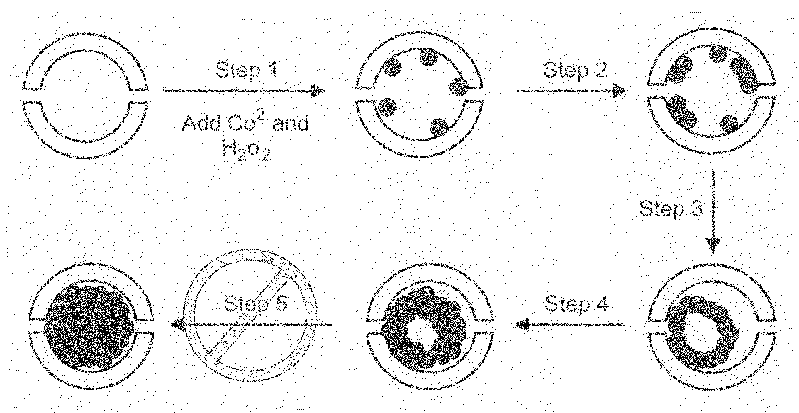
Fabrication of metal nanoshells
PatentInactiveUS20080014621A1
Innovation
- Employing apoferritin protein molecules in an aqueous solution as biotemplates to form hollow metal nanoparticles by reintroducing metal ions into the protein's hollow core, controlling the number of metal atoms to create stable metal nanoshells without forming solid particles.
Patent
Innovation
- Development of hybrid metal mesh structures combining different metals (e.g., gold, silver, copper) to enhance conductivity and optical transparency for nanotechnology applications.
- Novel fabrication techniques for ultra-thin metal mesh with sub-10nm feature sizes, enabling higher transparency while maintaining electrical conductivity.
- Implementation of hierarchical metal mesh structures with multi-scale features that optimize both mechanical flexibility and electrical performance for flexible electronics.
Environmental Impact and Sustainability Considerations
The integration of metal mesh structures in nanotechnology applications presents significant environmental implications that warrant careful consideration. As these materials become increasingly prevalent in various sectors, their environmental footprint throughout the lifecycle—from production to disposal—requires thorough assessment. The manufacturing processes for metal nanomeshes often involve energy-intensive methods and potentially hazardous chemicals, raising concerns about resource depletion and pollution.
Metal mesh nanomaterials exhibit unique properties that can contribute positively to environmental sustainability. Their application in advanced filtration systems demonstrates remarkable efficiency in removing contaminants from water and air, potentially addressing critical environmental challenges. Additionally, when incorporated into catalytic converters and renewable energy technologies, these materials can enhance performance while reducing the consumption of rare or precious metals, thereby conserving valuable natural resources.
However, the environmental fate of metal nanomeshes after disposal remains inadequately understood. The potential for these materials to release metal ions or nanoparticles into ecosystems poses risks of bioaccumulation and toxicity in aquatic and terrestrial organisms. Research indicates that certain metal nanomeshes may persist in the environment for extended periods, potentially disrupting ecological balances and food chains.
Sustainable design principles are increasingly being applied to metal mesh nanotechnology development. This includes exploring biodegradable substrates, implementing closed-loop manufacturing systems, and developing recovery methods for valuable metals. The concept of "green nanotechnology" emphasizes designing nanomaterials and their production processes to minimize environmental impact while maximizing beneficial applications, particularly in environmental remediation and clean energy generation.
Regulatory frameworks worldwide are evolving to address the unique environmental considerations associated with nanomaterials. These include specific guidelines for handling, disposal, and risk assessment of metal nanomeshes. The implementation of life cycle assessment (LCA) methodologies has become essential in evaluating the comprehensive environmental impact of these materials, from raw material extraction through manufacturing, use, and end-of-life management.
Industry-academic collaborations are driving innovation in environmentally responsible approaches to metal mesh nanotechnology. These partnerships focus on developing less toxic alternatives, improving energy efficiency in production, and creating effective recycling methodologies. The establishment of standardized testing protocols for environmental impact assessment represents a crucial step toward ensuring the sustainable integration of metal mesh nanotechnology into commercial applications.
Standardization and Quality Control Frameworks
The standardization and quality control of metal mesh in nanotechnology applications represent critical frameworks that ensure consistency, reliability, and reproducibility across research, development, and manufacturing processes. Currently, several international organizations including ISO (International Organization for Standardization), ASTM International, and IEEE have established working groups dedicated to developing comprehensive standards for nanomaterials, with specific attention to metal mesh structures. These standards address key parameters such as mesh aperture size, wire diameter uniformity, material purity, and surface characteristics.
Quality control protocols for metal mesh production typically involve multi-stage verification processes. Primary inspection utilizes high-resolution imaging techniques including scanning electron microscopy (SEM) and transmission electron microscopy (TEM) to verify structural integrity and dimensional accuracy at the nanoscale. Secondary verification employs spectroscopic methods such as X-ray photoelectron spectroscopy (XPS) and energy-dispersive X-ray spectroscopy (EDS) to confirm material composition and detect potential contaminants that could compromise performance.
Statistical process control (SPC) methodologies have been adapted specifically for nanomaterial production environments, enabling real-time monitoring of critical quality parameters during metal mesh fabrication. These systems typically implement six-sigma principles with modified control limits that account for the unique challenges of nanoscale manufacturing variability. Documentation requirements have also evolved to include detailed characterization of batch-to-batch consistency and traceability throughout the supply chain.
Certification frameworks for metal mesh in critical applications such as biomedical devices, semiconductor manufacturing, and aerospace components have become increasingly stringent. Third-party verification protocols now commonly require performance testing under simulated operational conditions, accelerated aging studies, and comprehensive documentation of manufacturing processes. The emergence of digital quality management systems has facilitated more robust tracking of quality metrics across global supply chains.
Harmonization efforts between different regional standards remain an ongoing challenge. The International Nanotechnology Standardization Roadmap has identified metal mesh standardization as a priority area, with particular focus on establishing universal terminology, measurement protocols, and performance benchmarks. Industry consortia have formed collaborative working groups to address these gaps, recognizing that standardization accelerates commercial adoption and reduces market barriers for emerging nanotechnology applications utilizing metal mesh components.
Unlock deeper insights with Patsnap Eureka Quick Research — get a full tech report to explore trends and direct your research. Try now!
Generate Your Research Report Instantly with AI Agent
Supercharge your innovation with Patsnap Eureka AI Agent Platform!