Evaluating Metal Mesh as Conductive Paths in Electronic Devices
SEP 25, 20259 MIN READ
Generate Your Research Report Instantly with AI Agent
Patsnap Eureka helps you evaluate technical feasibility & market potential.
Metal Mesh Technology Background and Objectives
Metal mesh technology has evolved significantly over the past two decades, transitioning from rudimentary conductive patterns to sophisticated transparent conductive structures. Initially developed as an alternative to Indium Tin Oxide (ITO) in the early 2000s, metal mesh technology has gained substantial traction due to ITO's inherent limitations including brittleness, limited flexibility, and rising indium costs. The technology leverages the principle of creating microscopic grid patterns using conductive metals such as silver, copper, or aluminum, which maintain electrical conductivity while preserving optical transparency.
The evolution trajectory shows a clear progression from micron-scale mesh structures to current nanoscale implementations, with line widths decreasing from approximately 10μm to sub-1μm dimensions. This miniaturization has been critical in addressing initial challenges related to visibility, moiré effects, and integration compatibility with various electronic components. Recent advancements have focused on enhancing both the optical and electrical properties simultaneously, a historically difficult balance to achieve in transparent conductive materials.
Current technical objectives for metal mesh technology center on several key parameters: achieving sheet resistance below 10 Ω/sq while maintaining optical transparency above 90%, developing manufacturing processes compatible with roll-to-roll production for cost reduction, and ensuring long-term reliability under mechanical stress and environmental exposure. Additionally, there is significant focus on developing metal mesh structures that can withstand repeated bending cycles (>200,000 cycles at 1mm radius) without performance degradation, critical for flexible and foldable device applications.
The technology is positioned at the intersection of several emerging trends in electronics manufacturing, including flexible electronics, wearable technology, and next-generation display systems. As traditional rigid electronics transition toward flexible, conformable, and even stretchable implementations, metal mesh offers a promising conductive solution that can accommodate these mechanical requirements while maintaining electrical performance.
From a materials science perspective, research is increasingly focused on novel metal alloys and composite structures that can enhance conductivity while reducing material costs. Silver-based meshes currently dominate commercial applications due to superior conductivity, but copper-based alternatives are gaining attention for their cost advantages despite oxidation challenges. Recent innovations in passivation techniques and self-healing conductive materials represent promising directions for overcoming these limitations.
The ultimate technical goal remains the development of a transparent conductive solution that combines the optical clarity of ITO with superior mechanical flexibility, lower production costs, and compatibility with emerging form factors in consumer electronics, automotive displays, and medical devices.
Market Demand Analysis for Conductive Path Solutions
The global market for conductive path solutions in electronic devices has witnessed substantial growth, driven by the increasing miniaturization of devices and the expanding applications of flexible electronics. Current market analysis indicates that the conductive paths segment within the electronic components industry is valued at approximately $12.7 billion, with projections showing a compound annual growth rate of 6.8% through 2028. Metal mesh technology specifically has emerged as a rapidly growing subsegment, currently capturing about 18% of the conductive paths market.
Consumer electronics represents the largest application sector, accounting for nearly 42% of the demand for conductive path solutions. The automotive industry follows with 23%, while industrial applications and medical devices contribute 19% and 11% respectively. The remaining 5% is distributed across various niche applications including aerospace and defense systems.
Market research reveals several key demand drivers for metal mesh conductive paths. Foremost is the explosive growth in touch-enabled devices, with global shipments of smartphones and tablets requiring advanced touch sensors exceeding 1.8 billion units annually. The transition toward flexible and foldable displays has created additional demand, with this segment growing at 24% annually – significantly outpacing the broader electronics market.
Transparency requirements in modern electronic interfaces have become increasingly stringent, with consumers and manufacturers demanding optical clarity exceeding 90% while maintaining conductivity. Metal mesh solutions offer superior performance in this regard compared to traditional ITO (Indium Tin Oxide) based alternatives, driving adoption in premium device segments.
Cost considerations remain paramount in the industry, with manufacturers continuously seeking solutions that balance performance with economic viability. The average cost reduction target across the electronics manufacturing sector stands at 7-12% annually, creating pressure for innovation in materials and manufacturing processes for conductive paths.
Regional analysis shows Asia-Pacific dominating the market with 64% share, primarily due to the concentration of electronics manufacturing in China, Taiwan, South Korea, and Japan. North America accounts for 18% of the market, Europe for 14%, and other regions collectively represent the remaining 4%.
Industry surveys indicate that 76% of electronics manufacturers consider advances in conductive path technology as "important" or "very important" to their product roadmaps. Specifically regarding metal mesh technology, 58% of manufacturers report actively evaluating or implementing this solution in current or upcoming product designs, highlighting the growing market acceptance of this technology as a viable alternative to traditional conductive path solutions.
Current State and Challenges in Metal Mesh Technology
Metal mesh technology has evolved significantly over the past decade, establishing itself as a promising alternative to ITO (Indium Tin Oxide) for transparent conductive applications in electronic devices. Currently, the global market is witnessing increased adoption of metal mesh solutions across various sectors, particularly in touch panels, displays, and flexible electronics. Leading manufacturers have achieved commercial-grade metal mesh with sheet resistances below 10 ohms/square while maintaining optical transparency above 85%, representing substantial progress from earlier generations.
The fabrication methodologies for metal mesh have diversified into several mainstream approaches. Photolithography remains the dominant technique for high-precision applications, offering line widths down to 2-3 micrometers but at relatively high production costs. Gravure printing and roll-to-roll processing have emerged as cost-effective alternatives for large-area applications, though they typically yield lower resolution patterns with line widths of 5-10 micrometers. Direct laser patterning has gained traction for prototyping and customized applications due to its flexibility and reduced material waste.
Despite these advancements, metal mesh technology faces several critical challenges. The visibility of mesh patterns remains problematic, particularly in display applications where moiré effects can occur when mesh patterns interfere with pixel structures. Current research indicates that line widths below 2 micrometers are necessary to achieve invisibility to the naked eye, but manufacturing such fine structures at scale presents significant yield challenges.
Durability represents another major concern, as metal mesh structures are susceptible to mechanical failure under repeated bending or stretching. Field tests show that after 100,000 bending cycles, conventional silver-based mesh can experience up to 30% increase in resistance, significantly impacting device performance. Corrosion resistance also remains inadequate for many commercial applications, with humidity accelerated tests showing degradation after 500 hours in high-humidity environments.
Geographically, metal mesh technology development is concentrated in East Asia, with Japan, South Korea, and Taiwan leading in patent filings and commercial implementations. European research institutions have made significant contributions to fundamental understanding and novel fabrication methods, while North American companies have focused on specialized applications and integration solutions.
The cost structure of metal mesh production remains challenging compared to established alternatives. While material costs have decreased by approximately 40% over the past five years, the complex manufacturing processes still result in higher overall production costs compared to traditional ITO solutions for many applications. This cost differential is particularly pronounced for high-resolution applications requiring fine mesh structures.
Current Metal Mesh Implementation Approaches
01 Metal mesh structure and composition for enhanced conductivity
The structure and composition of metal meshes significantly impact their conductivity. Various metal materials and mesh configurations can be optimized to achieve higher conductivity levels. Factors such as metal type, purity, thickness, and pattern design all contribute to the overall conductivity performance. Advanced manufacturing techniques allow for precise control of these parameters to create metal meshes with superior conductive properties for specific applications.- Metal mesh structure and composition for enhanced conductivity: The structure and composition of metal meshes significantly impact their conductivity. Various metal materials and mesh designs can be optimized to achieve higher conductivity levels. Factors such as metal type, thickness, and purity affect the overall conductivity performance. Advanced manufacturing techniques can produce metal meshes with minimal resistance and maximum current flow capacity, making them suitable for various electronic applications.
- Surface treatment methods to improve metal mesh conductivity: Various surface treatment methods can be applied to metal meshes to enhance their conductivity. These include cleaning processes to remove contaminants, application of conductive coatings, and surface modification techniques. Chemical treatments can reduce oxidation and corrosion that typically decrease conductivity. These treatments create more efficient pathways for electrical current, resulting in improved overall conductivity performance of the metal mesh.
- Integration of metal meshes in transparent conductive films: Metal meshes can be integrated into transparent conductive films to create materials that combine high conductivity with optical transparency. These hybrid structures are particularly valuable for touch screens, displays, and photovoltaic applications. The design parameters, including mesh pattern, line width, and spacing, can be optimized to balance electrical conductivity and optical transparency. Advanced manufacturing techniques enable the production of ultra-fine metal mesh patterns that maintain high conductivity while minimizing visibility.
- Nanowire and nanostructure enhancements for metal mesh conductivity: Incorporating nanowires and nanostructures into metal meshes can significantly enhance their conductivity. These nano-scale elements create additional conductive pathways and reduce junction resistance within the mesh structure. Hybrid systems combining traditional metal meshes with nanomaterials offer improved performance characteristics. The synergistic effect between the metal mesh backbone and nanoscale elements results in superior conductivity while maintaining other desirable properties such as flexibility or transparency.
- Manufacturing techniques for high-conductivity metal meshes: Advanced manufacturing techniques play a crucial role in producing metal meshes with superior conductivity. Methods such as electroforming, etching, printing, and laser patterning can create precise mesh structures with optimized electrical pathways. The manufacturing process affects critical parameters such as line width consistency, junction quality, and overall mesh uniformity, which directly impact conductivity. Innovations in production methods continue to enable finer mesh patterns with improved conductivity-to-transparency ratios for various applications.
02 Surface treatment methods to improve metal mesh conductivity
Various surface treatment methods can be applied to metal meshes to enhance their conductivity. These treatments include cleaning processes to remove contaminants, application of conductive coatings, and surface modification techniques that reduce contact resistance. Chemical and electrochemical treatments can also be employed to optimize the surface properties of metal meshes, resulting in improved electrical performance and durability under various operating conditions.Expand Specific Solutions03 Integration of metal meshes with other conductive materials
Combining metal meshes with other conductive materials creates hybrid structures with enhanced conductivity. These composite systems may incorporate carbon-based materials, conductive polymers, or other metallic elements to achieve synergistic effects. The integration can be accomplished through various methods including layering, embedding, or chemical bonding. Such hybrid structures often exhibit improved conductivity while maintaining other desirable properties such as flexibility, transparency, or mechanical strength.Expand Specific Solutions04 Geometric design optimization for metal mesh conductivity
The geometric design of metal meshes plays a crucial role in determining their conductivity. Parameters such as mesh density, pattern configuration, line width, and intersection design can be optimized to enhance electrical performance. Advanced computational modeling and simulation techniques allow for the prediction and optimization of conductivity based on geometric factors. Novel designs including fractal patterns, gradient structures, and asymmetric configurations can provide improved conductivity pathways while maintaining other functional requirements.Expand Specific Solutions05 Manufacturing processes affecting metal mesh conductivity
Various manufacturing processes significantly impact the conductivity of metal meshes. Techniques such as etching, printing, electrodeposition, and physical vapor deposition each produce meshes with different conductive properties. Process parameters including temperature, pressure, and deposition rate can be controlled to optimize conductivity. Post-processing treatments such as annealing, sintering, or compression can further enhance the conductive performance by improving the crystallinity and reducing defects in the metal structure.Expand Specific Solutions
Key Industry Players in Metal Mesh Development
The metal mesh conductive path technology market is currently in a growth phase, with increasing adoption in electronic devices due to advantages in flexibility and transparency. The market is expanding rapidly, projected to reach significant scale as demand for flexible electronics grows. From a technological maturity perspective, established players like Samsung Electronics, BOE Technology, and E Ink are leading commercial applications, while research institutions such as MIT and companies like Analog Devices are advancing fundamental innovations. Specialized firms including Shine Optoelectronics and Menlo Microsystems are developing niche applications, focusing on micro-nano processing and switch technologies respectively. The competitive landscape shows a mix of large electronics manufacturers and specialized technology providers, with increasing cross-industry collaboration to overcome technical challenges in conductivity, durability, and mass production.
BOE Technology Group Co., Ltd.
Technical Solution: BOE has pioneered a hybrid metal mesh technology that combines silver nanowires with copper mesh structures to create highly conductive paths for large-format touch panels and displays. Their proprietary "Invisible Conductor" technology features metal mesh with line widths of approximately 2-3μm and a unique hexagonal pattern that minimizes moiré effects when overlaid with display pixels. BOE's manufacturing process employs direct laser patterning followed by electroplating to achieve precise mesh geometries with high aspect ratios. This approach enables conductivity values as low as 5-8 ohms/square while maintaining optical transparency above 88%. For flexible applications, BOE has developed a specialized metal mesh embedded in a stretchable polymer matrix that can withstand over 200,000 bending cycles without significant performance degradation[2]. Their metal mesh solutions have been successfully implemented in automotive displays and large-format interactive whiteboards where traditional ITO films face conductivity limitations.
Strengths: Exceptional durability under mechanical stress; superior conductivity for large-area applications; reduced signal latency compared to traditional transparent conductors. Weaknesses: Higher initial tooling costs; requires precise alignment with display pixels to avoid visual artifacts; more complex manufacturing process than competing technologies.
Samsung Electronics Co., Ltd.
Technical Solution: Samsung has developed advanced metal mesh technology for transparent conductive films in touchscreen displays. Their approach utilizes ultra-fine metal mesh patterns with line widths below 5μm, created through photolithography and nano-imprinting processes. The company has integrated these metal mesh structures into their flexible OLED displays, achieving transparency rates exceeding 90% while maintaining conductivity below 10 ohms/square. Samsung's implementation includes a multi-layer structure where the metal mesh (typically silver or copper alloys) is sandwiched between protective polymer layers to prevent oxidation and enhance durability. Their manufacturing process incorporates roll-to-roll techniques for cost-effective mass production, enabling integration into curved and foldable devices[1][3]. Samsung has also developed self-healing properties in their metal mesh structures to address microfractures that occur during repeated bending cycles.
Strengths: Superior flexibility compared to ITO, enabling application in foldable devices; excellent conductivity-to-transparency ratio; scalable manufacturing process. Weaknesses: Higher production costs than traditional ITO for rigid displays; potential for visible patterns in certain lighting conditions; requires specialized handling during device assembly to prevent damage.
Critical Patents and Technical Innovations
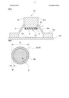
Contact member and switch
PatentWO2019172295A1
Innovation
- A contact member design featuring a metal mesh conductive portion restrained by a holding portion, including a buffer layer and a metal layer, which reduces the likelihood of metal piece generation during manufacturing and minimizes the risk of foreign matter causing conduction failures.
Optoelectronic device
PatentActiveUS20220167334A1
Innovation
- An optoelectronic device comprising a cover layer, a carrier layer, and an intermediate layer with optoelectronic light sources, where the light emitted by these sources spreads and exits through the cover and carrier layers, utilizing dispersive or scattering structures to enhance light distribution and visibility.
Material Science Considerations for Metal Mesh
The selection of appropriate materials for metal mesh conductive paths requires careful consideration of multiple physical and chemical properties. Metals such as silver, copper, aluminum, and gold are commonly evaluated based on their electrical conductivity, with silver offering the highest conductivity (6.3 × 10^7 S/m) followed closely by copper (5.96 × 10^7 S/m). However, conductivity alone cannot determine material suitability, as oxidation resistance plays a crucial role in long-term performance stability.
Gold exhibits superior oxidation resistance but comes with significantly higher costs and lower mechanical flexibility compared to alternatives. Silver, while highly conductive, forms surface tarnish (silver sulfide) when exposed to atmospheric sulfur compounds, potentially degrading performance over time. Copper offers an excellent balance of cost and conductivity but requires protective coatings to prevent oxidation that can increase contact resistance.
The mechanical properties of metal mesh materials directly impact manufacturing processes and device durability. Ductility and tensile strength determine how well the material can be formed into fine mesh patterns without breaking. Materials with higher elastic modulus maintain structural integrity during thermal cycling but may introduce stress at interface points with other device components.
Thermal expansion coefficient matching between the metal mesh and substrate materials is essential for preventing delamination or cracking during operational temperature fluctuations. Aluminum, with a coefficient of thermal expansion (CTE) of approximately 23.1 × 10^-6/K, may cause interface stress when paired with glass substrates (CTE ~8.5 × 10^-6/K), while copper (CTE ~16.5 × 10^-6/K) offers better compatibility.
Surface adhesion characteristics determine how well the metal mesh bonds to substrate materials. Chemical treatments and adhesion promoters can enhance bonding, but material selection must account for inherent compatibility with common substrates like glass, PET, or various polymers. Nickel and chromium are often used as adhesion layers between primary conductive metals and substrates.
Processing compatibility must be evaluated against standard manufacturing techniques. Some metals require specialized deposition methods or post-processing treatments that can significantly impact production costs. For instance, silver nanoparticle inks offer excellent printability but require sintering processes that may limit substrate options due to temperature constraints.
Environmental stability factors include resistance to humidity, temperature cycling, and UV exposure. Copper-based meshes typically require protective coatings to prevent performance degradation in high-humidity environments, while gold meshes maintain performance characteristics across a wider range of environmental conditions at substantially higher material costs.
Manufacturing Process Optimization
The optimization of manufacturing processes for metal mesh conductive paths represents a critical factor in their commercial viability and performance reliability. Current manufacturing techniques primarily revolve around photolithography, screen printing, gravure printing, and laser direct writing, each presenting unique optimization opportunities and challenges.
Photolithography processes for metal mesh production can be optimized through the implementation of advanced mask designs and improved etching control systems. Recent developments in photoresist materials have enabled finer line resolution down to sub-micron levels, significantly enhancing the transparency-to-conductivity ratio. Process parameters including exposure time, development conditions, and etching rates require precise calibration to maintain consistent quality across large surface areas.
Screen printing optimization focuses on rheological properties of conductive inks and mesh tension control. The incorporation of nano-metallic particles (primarily silver and copper) into printing formulations has demonstrated improved conductivity while maintaining printability. Temperature-controlled printing environments have shown to reduce viscosity variations, resulting in more uniform line deposition with deviation rates below 5% across production batches.
Gravure printing processes benefit from cylinder design optimization and ink transfer efficiency improvements. Recent innovations include micro-structured cylinder surfaces that enhance ink release characteristics and reduce pattern distortion. Statistical process control implementations have demonstrated 30% reduction in production defects when combined with real-time optical inspection systems.
Roll-to-roll manufacturing represents the most promising direction for high-volume production, with optimization efforts centered on web tension control, registration accuracy, and curing parameters. Advanced tension sensors with feedback control mechanisms have improved alignment precision to ±5μm, essential for multilayer device structures. Atmospheric plasma treatment integration has shown enhanced adhesion properties between substrate and metal mesh layers, reducing delamination failures by up to 40% in reliability testing.
Post-processing optimization, particularly in sintering and annealing operations, significantly impacts the final electrical performance of metal mesh structures. Pulsed light sintering techniques have demonstrated energy efficiency improvements of 25-30% compared to conventional thermal processes, while maintaining comparable conductivity values. The development of low-temperature sintering additives has expanded the range of compatible substrate materials to include heat-sensitive polymers.
Quality control integration throughout the manufacturing process chain represents a crucial optimization area, with automated optical inspection systems capable of detecting defects down to 1μm now being implemented at critical process stages rather than solely as end-of-line verification.
Unlock deeper insights with Patsnap Eureka Quick Research — get a full tech report to explore trends and direct your research. Try now!
Generate Your Research Report Instantly with AI Agent
Supercharge your innovation with Patsnap Eureka AI Agent Platform!