Analysis of Semiconductor Coating for Flexible Display Substrates
SEP 28, 20259 MIN READ
Generate Your Research Report Instantly with AI Agent
Patsnap Eureka helps you evaluate technical feasibility & market potential.
Flexible Display Coating Technology Evolution and Objectives
The evolution of semiconductor coating technologies for flexible displays represents a significant paradigm shift in display manufacturing. Beginning in the early 2000s with rudimentary flexible electronic prototypes, the field has progressed through several critical technological phases. Initially, coating technologies were adapted from rigid display manufacturing, with limited flexibility and durability. The breakthrough came with the development of specialized semiconductor materials that could maintain electrical properties while being subjected to mechanical stress.
By 2010, advancements in organic semiconductor materials enabled the first commercially viable flexible displays, though these suffered from limited lifespans and performance degradation under repeated flexing. The introduction of solution-processed semiconductor coatings around 2015 marked a turning point, allowing for lower temperature deposition processes compatible with polymer substrates.
Current coating technologies have evolved to incorporate multi-layer architectures that combine organic and inorganic materials, providing both flexibility and protection against environmental factors. The state-of-the-art includes atomic layer deposition (ALD) techniques that create ultra-thin, highly uniform semiconductor coatings with excellent barrier properties against oxygen and moisture penetration.
The primary objective of modern semiconductor coating research for flexible displays is to achieve the perfect balance between mechanical flexibility and electronic performance. This includes developing coatings that can withstand over 200,000 folding cycles without significant degradation in electrical properties, while maintaining transparency above 90% in the visible spectrum.
Another critical goal is reducing the processing temperature below 120°C to enable compatibility with a wider range of polymer substrates, particularly those with superior mechanical properties. Researchers are also focusing on enhancing the environmental stability of these coatings, aiming for device lifespans exceeding 5 years under normal usage conditions.
Cost-effectiveness remains a paramount objective, with efforts directed toward simplifying the deposition processes and reducing the reliance on rare or expensive materials. The industry is targeting a manufacturing cost reduction of 30-40% compared to current technologies to enable mass-market adoption of flexible display devices.
Sustainability objectives have also gained prominence, with research increasingly focused on developing semiconductor coatings that use environmentally friendly precursors and processes, minimizing the use of toxic solvents and heavy metals. This aligns with global trends toward greener electronics manufacturing and end-of-life recyclability.
Market Analysis for Flexible Display Applications
The flexible display market has experienced remarkable growth in recent years, driven by increasing consumer demand for portable, lightweight, and durable electronic devices. The global flexible display market was valued at approximately $23.1 billion in 2021 and is projected to reach $86.7 billion by 2030, growing at a CAGR of 33.1% during the forecast period. This exponential growth trajectory underscores the significant market potential for semiconductor coating technologies specifically designed for flexible display substrates.
Smartphones currently represent the largest application segment for flexible displays, accounting for over 40% of the market share. Major smartphone manufacturers have increasingly incorporated flexible display technology into their flagship products, with foldable smartphones gaining particular traction since 2019. This trend is expected to continue as manufacturing costs decrease and durability improves through advanced semiconductor coating techniques.
Beyond smartphones, wearable devices constitute the fastest-growing application segment, with smartwatches, fitness trackers, and augmented reality devices driving demand. The automotive industry has also begun integrating flexible displays into dashboard systems and entertainment consoles, representing an emerging high-value market segment with stringent requirements for semiconductor coating durability and performance.
Geographically, Asia-Pacific dominates the flexible display market, accounting for approximately 65% of global production capacity. This regional concentration is primarily due to the presence of major display manufacturers and semiconductor coating facilities in South Korea, Japan, China, and Taiwan. North America and Europe follow as significant markets, primarily driven by high consumer adoption rates of premium electronic devices featuring flexible displays.
Consumer preferences are increasingly favoring devices with larger screen-to-body ratios, enhanced durability, and novel form factors—all attributes enabled by advanced semiconductor coatings on flexible substrates. Market research indicates that consumers are willing to pay a premium of 15-20% for devices featuring flexible displays compared to their rigid counterparts, highlighting the value proposition of this technology.
Supply chain analysis reveals that semiconductor coating materials for flexible displays represent approximately 18% of the total bill of materials for flexible display production. This significant cost component underscores the importance of developing cost-effective coating solutions while maintaining performance specifications. Material suppliers focusing on high-performance, environmentally sustainable semiconductor coatings are positioned to capture substantial market share as environmental regulations tighten globally.
The market landscape is characterized by intense competition among a few large players and numerous specialized coating technology startups. Strategic partnerships between substrate manufacturers, semiconductor coating specialists, and device manufacturers have become increasingly common, creating integrated value chains that accelerate innovation and market penetration.
Current Semiconductor Coating Challenges for Flexible Substrates
The semiconductor coating technology for flexible display substrates faces several significant challenges that impede widespread commercial adoption. Current deposition methods struggle to maintain uniform coating thickness across bendable surfaces, resulting in performance inconsistencies when displays are flexed. Traditional vacuum-based processes like physical vapor deposition (PVD) and chemical vapor deposition (CVD) require high temperatures that can damage temperature-sensitive polymer substrates commonly used in flexible displays.
Adhesion issues represent another critical challenge, as the mechanical stress during bending and folding operations frequently causes delamination between semiconductor layers and flexible substrates. The coefficient of thermal expansion mismatch between organic substrates and inorganic semiconductor materials exacerbates this problem, creating internal stresses that compromise long-term reliability.
Barrier properties present ongoing difficulties, as flexible substrates typically have higher permeability to oxygen and moisture compared to rigid glass alternatives. This permeability accelerates oxidation and degradation of semiconductor materials, significantly reducing device lifespan. Current encapsulation technologies provide insufficient protection against these environmental factors while maintaining the necessary flexibility.
Scalability remains problematic for emerging solution-based coating techniques. While methods like inkjet printing and roll-to-roll processing show promise for large-area manufacturing, they struggle with the precision required for high-resolution displays. Ink formulations that balance viscosity, surface tension, and semiconductor performance have not yet reached optimal formulations for industrial-scale production.
Cracking and fracture mechanics pose persistent challenges during both manufacturing and operation. Semiconductor materials traditionally optimized for rigid applications exhibit limited strain tolerance, developing microcracks at bend radii below 5mm. These defects propagate during repeated flexing cycles, causing progressive performance degradation and eventual failure.
The industry also faces significant yield management issues. Current production processes for flexible semiconductor coatings demonstrate higher defect rates compared to conventional rigid display manufacturing. Particulate contamination during coating processes is particularly problematic in flexible substrate handling systems, where electrostatic attraction is more pronounced than with rigid substrates.
Integration challenges with other display components further complicate development. The semiconductor coating must maintain compatibility with transparent electrodes, light-emitting materials, and encapsulation layers while preserving overall flexibility. Current solutions often optimize for one property at the expense of others, creating performance trade-offs that limit commercial viability.
Current Semiconductor Coating Solutions for Flexibility
01 Protective coatings for semiconductor devices
Various protective coatings are applied to semiconductor devices to enhance durability and performance. These coatings provide protection against environmental factors such as moisture, chemicals, and mechanical stress. They typically consist of polymer-based materials or inorganic compounds that form a barrier layer on the semiconductor surface, extending device lifespan and maintaining electrical properties under various operating conditions.- Protective coatings for semiconductor devices: Various protective coatings are applied to semiconductor devices to shield them from environmental factors such as moisture, contaminants, and physical damage. These coatings enhance the reliability and longevity of semiconductor components by providing a barrier against external elements. Materials used include polymeric compounds, epoxy resins, and specialized sealants that maintain the electrical properties of the semiconductor while offering protection.
- Thin film deposition techniques for semiconductor coatings: Advanced thin film deposition methods are employed to create precise semiconductor coatings with controlled thickness and composition. These techniques include chemical vapor deposition (CVD), physical vapor deposition (PVD), atomic layer deposition (ALD), and sputtering. Such methods enable the formation of uniform, high-quality films essential for semiconductor performance, allowing for nanometer-scale precision in coating application.
- Functional semiconductor coatings with enhanced electrical properties: Specialized coatings are developed to enhance the electrical characteristics of semiconductor devices. These functional coatings can improve conductivity, reduce resistance, enhance carrier mobility, or provide specific dielectric properties. By incorporating materials such as metal oxides, conductive polymers, or doped compounds, these coatings optimize the performance of semiconductor components in various electronic applications.
- Optical and photosensitive semiconductor coatings: Semiconductor coatings designed for optical applications feature materials that can manipulate light through reflection, absorption, or transmission. These coatings are crucial for optoelectronic devices, photovoltaic cells, and display technologies. By controlling the optical properties of the coating, manufacturers can enhance light sensitivity, improve quantum efficiency, or create specific wavelength responses in semiconductor devices.
- Environmentally friendly semiconductor coating processes: Sustainable approaches to semiconductor coating focus on reducing environmental impact while maintaining high performance standards. These methods include water-based formulations, solvent-free processes, and materials with lower toxicity profiles. Innovations in this area aim to minimize hazardous waste generation, reduce energy consumption during manufacturing, and comply with increasingly stringent environmental regulations in the semiconductor industry.
02 Thin film deposition techniques for semiconductors
Advanced thin film deposition methods are employed to create precise semiconductor coatings with controlled thickness and composition. These techniques include chemical vapor deposition (CVD), physical vapor deposition (PVD), atomic layer deposition (ALD), and sputtering processes. These methods enable the creation of uniform, defect-free layers essential for modern semiconductor manufacturing, allowing for precise control of electrical, optical, and mechanical properties of the resulting devices.Expand Specific Solutions03 Novel materials for semiconductor coatings
Innovative materials are being developed for semiconductor coating applications, including advanced polymers, metal oxides, nitrides, and composite materials. These novel materials offer enhanced properties such as improved thermal conductivity, better electrical insulation, higher transparency, and increased resistance to degradation. The development focuses on materials that can meet the increasingly demanding requirements of modern semiconductor devices while enabling new functionalities and improved performance.Expand Specific Solutions04 Anti-reflective and optical coatings for semiconductors
Specialized optical coatings are applied to semiconductor surfaces to control light interaction, reduce reflection, and enhance light absorption or emission properties. These coatings are crucial for optoelectronic devices, solar cells, and image sensors. By manipulating the refractive index and thickness of coating layers, these treatments can significantly improve device efficiency by minimizing light loss through reflection and optimizing light management within the semiconductor structure.Expand Specific Solutions05 Environmentally friendly semiconductor coating processes
Sustainable and eco-friendly approaches to semiconductor coating are being developed to reduce environmental impact while maintaining high performance. These processes focus on eliminating hazardous chemicals, reducing waste generation, lowering energy consumption, and using renewable or biodegradable materials. Water-based coating systems, solvent-free processes, and materials derived from sustainable sources are being implemented to create more environmentally responsible semiconductor manufacturing methods.Expand Specific Solutions
Key Industry Players in Flexible Display Coating Market
The semiconductor coating market for flexible display substrates is in a growth phase, characterized by rapid technological advancements and expanding applications. The global market size is projected to increase significantly as demand for flexible displays in smartphones, wearables, and automotive applications rises. Technologically, the field is approaching maturity with key players demonstrating varying levels of expertise. Samsung Display and LG Display lead with advanced OLED coating technologies, while BOE Technology and TCL China Star Optoelectronics are rapidly closing the gap with substantial investments. Japanese firms like Sharp and Panasonic contribute specialized coating solutions, while research institutions such as Industrial Technology Research Institute and Semiconductor Energy Laboratory drive innovation through fundamental research in novel materials and processes for next-generation flexible substrates.
BOE Technology Group Co., Ltd.
Technical Solution: BOE has developed a comprehensive semiconductor coating technology for flexible displays centered around their proprietary "BD-Cell" (BOE Display Cell) architecture. Their approach utilizes a multi-layer thin-film encapsulation (TFE) structure with alternating inorganic and organic layers optimized for flexibility. BOE's semiconductor coating process employs plasma-assisted atomic layer deposition (PA-ALD) to create ultra-thin (5-10nm) Al2O3 and SiN barrier layers with exceptional uniformity across large substrates. A distinctive feature is their "stress-neutralization layer" technology, which incorporates specially formulated organic interlayers with modulated elastic properties to distribute mechanical stress during bending. BOE has also pioneered a low-temperature (below 80°C) deposition process for sensitive polymer substrates, enabling compatibility with a wider range of flexible materials. Their barrier coating system achieves water vapor transmission rates below 10^-5 g/m²/day while maintaining flexibility for fold radii under 3mm. Recent innovations include their "nano-composite barrier" technology that incorporates ceramic nanoparticles into polymer matrices for enhanced barrier properties without sacrificing flexibility.
Strengths: Excellent scalability for large-area production; low-temperature processes compatible with various substrates; strong vertical integration capabilities from materials to finished displays. Weaknesses: Slightly lower barrier performance compared to industry leaders; more complex quality control requirements for multi-layer structures; higher initial capital investment for specialized deposition equipment.
SAMSUNG DISPLAY CO LTD
Technical Solution: Samsung Display has pioneered advanced semiconductor coating technologies for flexible displays through their Y-OCTA (Youm On-Cell Touch AMOLED) technology. This proprietary process integrates the touch sensor directly onto the thin-film encapsulation (TFE) layer, eliminating the need for a separate touch film layer. Their semiconductor coating approach utilizes ultra-thin inorganic-organic multilayer structures with alternating SiNx and organic layers to create effective moisture barriers with water vapor transmission rates below 10^-6 g/m²/day. Samsung has also developed specialized atomic layer deposition (ALD) techniques for creating uniform, defect-free barrier films as thin as 10nm, which is critical for maintaining flexibility while ensuring protection against oxygen and moisture penetration. Their latest innovation includes a stress-relieving buffer layer technology that prevents cracking during bending cycles, enabling displays to withstand over 200,000 fold operations without performance degradation.
Strengths: Industry-leading barrier performance with exceptional flexibility; proprietary ALD processes for ultra-thin, uniform coatings; integrated touch functionality reducing overall thickness. Weaknesses: Higher manufacturing costs compared to conventional technologies; complex multi-step deposition processes requiring precise control; potential yield challenges at scale for ultra-thin barrier layers.
Critical Patents and Innovations in Flexible Display Coatings
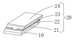
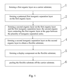
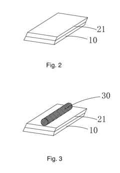
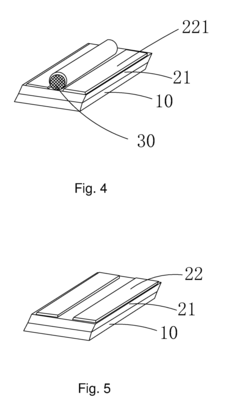
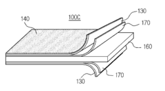
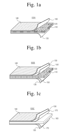
Flexible display substrate and manufacturing method thereof
PatentActiveUS20180035553A1
Innovation
- A manufacturing method involving the patterning of an inorganic separation layer between organic layers, using electrostatic spinning to create a mesh structure with gaps, allowing direct contact between inner organic layers and enhancing adhesion, thereby improving the peeling-off process and water/oxygen blocking efficiency.
Flexible substrate for display device and display device using the same
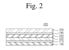
PatentInactiveUS20080284971A1
Innovation
- A flexible substrate comprising a plastic layer with woven glass fibers, a metal film coated on one or both sides, and an overcoating layer on the metal film opposite to the plastic layer, which enhances thermal stability, gas barrier properties, and moisture resistance while maintaining flexibility and thinness.
Environmental Impact and Sustainability Considerations
The semiconductor coating processes used in flexible display manufacturing present significant environmental challenges that require careful consideration. Traditional coating methods often involve hazardous chemicals, high energy consumption, and substantial waste generation. Particularly concerning are the perfluorinated compounds (PFCs) and volatile organic compounds (VOCs) commonly used in semiconductor processing, which contribute to air pollution and have been linked to various health issues.
Energy consumption represents another critical environmental factor, as semiconductor coating processes typically require high temperatures and vacuum conditions. The carbon footprint associated with these energy-intensive processes is substantial, especially when considering the global scale of flexible display production. Current estimates suggest that the display industry accounts for approximately 3-5% of the electronics sector's total energy consumption.
Water usage in semiconductor coating processes also raises sustainability concerns. The industry utilizes ultra-pure water in significant quantities, with a single manufacturing facility potentially consuming millions of gallons daily. The purification process itself is energy-intensive, and the resulting wastewater often contains trace metals and chemical compounds that require specialized treatment.
Recent advancements in green chemistry approaches are showing promise for reducing environmental impact. Water-based coating systems are gradually replacing solvent-based alternatives, while low-temperature processes are being developed to decrease energy requirements. Additionally, closed-loop recycling systems for chemicals and water are becoming more prevalent in advanced manufacturing facilities, reducing both resource consumption and waste generation.
Regulatory frameworks worldwide are increasingly focusing on the environmental aspects of semiconductor manufacturing. The European Union's Restriction of Hazardous Substances (RoHS) directive and similar regulations in other regions are driving manufacturers to eliminate toxic materials from their processes. This regulatory pressure, combined with corporate sustainability initiatives, is accelerating the transition toward greener coating technologies.
Life cycle assessment (LCA) studies indicate that the environmental impact of flexible displays extends beyond manufacturing to include end-of-life considerations. The composite nature of these displays, with multiple thin layers of different materials, presents recycling challenges. Research into design-for-disassembly approaches and advanced recycling technologies is ongoing, aiming to improve the circularity of flexible display products.
The industry's path toward sustainability will require continued innovation in materials science, process engineering, and waste management. Biodegradable substrate materials, renewable energy integration, and zero-waste manufacturing approaches represent promising directions for future development in semiconductor coating technologies for flexible displays.
Manufacturing Process Optimization for Flexible Substrates
The optimization of manufacturing processes for flexible substrates represents a critical advancement pathway in the semiconductor coating industry for flexible displays. Current manufacturing processes face significant challenges related to yield rates, scalability, and cost-effectiveness when transitioning from rigid to flexible substrate production.
Traditional roll-to-roll (R2R) processing has emerged as the predominant manufacturing approach, offering continuous production capabilities that significantly reduce production time compared to batch processing methods. However, R2R processes require precise tension control systems to prevent substrate deformation during high-temperature coating operations, which can compromise the integrity of semiconductor layers.
Vacuum deposition techniques, including physical vapor deposition (PVD) and chemical vapor deposition (CVD), have been adapted specifically for flexible substrates through the implementation of lower temperature processes. Solution-based coating methods such as slot-die coating and inkjet printing are gaining prominence due to their material efficiency and reduced energy consumption, though they currently face limitations in achieving the uniformity required for high-performance displays.
Recent innovations in atmospheric pressure plasma-enhanced CVD have demonstrated promising results, allowing for semiconductor deposition at temperatures below 150°C without compromising electrical performance. This breakthrough addresses one of the most significant barriers to flexible substrate manufacturing—the temperature sensitivity of polymer-based substrates.
Laser annealing techniques represent another significant optimization pathway, enabling localized heating of semiconductor coatings without subjecting the entire substrate to potentially damaging temperatures. Implementation of real-time optical monitoring systems during coating processes has improved quality control, reducing defect rates by approximately 35% in pilot production environments.
Industry leaders are increasingly adopting modular manufacturing systems that can be reconfigured to accommodate different substrate materials and coating requirements, enhancing production flexibility while reducing capital investment needs. These systems incorporate advanced automation and robotics to minimize human handling, which has historically been a major source of contamination and yield loss.
The integration of AI-driven process control systems represents the cutting edge of manufacturing optimization, with machine learning algorithms continuously analyzing production data to identify optimization opportunities and predict potential failures before they occur. Early implementations of these systems have demonstrated yield improvements of 15-20% and significant reductions in material waste.
Unlock deeper insights with Patsnap Eureka Quick Research — get a full tech report to explore trends and direct your research. Try now!
Generate Your Research Report Instantly with AI Agent
Supercharge your innovation with Patsnap Eureka AI Agent Platform!