Why Flexible Display Substrates Enhance Semiconductor Performance
SEP 28, 20259 MIN READ
Generate Your Research Report Instantly with AI Agent
PatSnap Eureka helps you evaluate technical feasibility & market potential.
Flexible Display Technology Evolution and Objectives
Flexible display technology has evolved significantly over the past two decades, transforming from conceptual research to commercial reality. The journey began in the early 2000s with rudimentary prototypes featuring limited flexibility and poor durability. These early displays utilized organic light-emitting diodes (OLEDs) on modified glass substrates, offering minimal bending capabilities while suffering from rapid performance degradation.
By 2010, the introduction of plastic substrates marked a critical turning point, enabling displays to achieve greater flexibility without compromising electronic performance. Polyimide emerged as a preferred substrate material due to its excellent thermal stability, chemical resistance, and mechanical properties. This advancement facilitated the development of displays that could be bent repeatedly without significant deterioration in semiconductor functionality.
The period between 2015 and 2020 witnessed remarkable progress in manufacturing techniques, particularly in low-temperature polysilicon (LTPS) and oxide thin-film transistor (TFT) technologies. These innovations allowed for the creation of high-performance semiconductors on flexible substrates, achieving electron mobility comparable to rigid displays while maintaining flexibility. Concurrently, encapsulation technologies evolved to protect sensitive electronic components from oxygen and moisture, substantially extending device lifespan.
Current flexible display technology employs ultrathin substrates measuring less than 100 micrometers, incorporating advanced semiconductor materials that maintain performance integrity even when subjected to mechanical stress. The neutral plane design concept has been instrumental in minimizing strain on semiconductor layers during flexing operations, thereby preserving electrical characteristics and extending operational longevity.
The primary objective of flexible display substrate development is to enhance semiconductor performance while maintaining mechanical flexibility. This involves achieving higher electron mobility, lower power consumption, and improved thermal management compared to conventional rigid displays. Additionally, researchers aim to develop substrates that can withstand repeated bending cycles exceeding 200,000 times without significant performance degradation.
Future technological goals include developing substrates capable of supporting stretchable electronics that can expand by at least 20% while maintaining semiconductor functionality. There is also significant focus on creating biodegradable flexible substrates to address environmental concerns associated with electronic waste. The ultimate vision encompasses fully transparent, self-healing substrates that automatically repair microcracks formed during mechanical deformation, thereby extending device lifespan and reliability in real-world applications.
Market Demand Analysis for Flexible Semiconductor Displays
The flexible display market has witnessed remarkable growth in recent years, driven by increasing consumer demand for portable, durable, and innovative electronic devices. Market research indicates that the global flexible display market is projected to reach $42.85 billion by 2027, growing at a CAGR of 28.1% from 2020 to 2027. This substantial growth reflects the expanding applications of flexible semiconductor displays across multiple industries.
Consumer electronics represents the largest market segment, with smartphones and wearable devices leading adoption. Major smartphone manufacturers have introduced foldable devices featuring flexible displays, creating a premium market segment that commands higher profit margins. The wearable technology sector has similarly embraced flexible displays, with smartwatches and fitness trackers benefiting from displays that conform to the human body.
Automotive applications represent another significant growth area. Curved dashboard displays and entertainment systems are increasingly common in mid-range and luxury vehicles. Market analysis suggests that by 2025, over 60% of new premium vehicles will incorporate some form of flexible display technology, representing a substantial opportunity for semiconductor manufacturers.
Healthcare and medical devices constitute an emerging but rapidly growing market segment. Flexible displays enable the development of wearable health monitors that can continuously track vital signs while conforming to the body's contours. The medical wearables market is expected to grow at 24.7% CAGR through 2026, with flexible display technology playing a crucial role in this expansion.
Regional analysis reveals Asia-Pacific as the dominant manufacturing hub, while North America leads in technology development and innovation. Europe shows strong growth potential, particularly in automotive and healthcare applications. China has made significant investments in flexible display manufacturing capacity, challenging the traditional dominance of South Korean and Japanese manufacturers.
Market barriers include high production costs and technical challenges in scaling manufacturing processes. The average production cost for flexible displays remains approximately 30% higher than rigid alternatives, though this gap is narrowing as manufacturing techniques improve and economies of scale develop.
Consumer surveys indicate strong preference for devices with flexible displays, with 72% of respondents expressing willingness to pay a premium for foldable smartphones. Durability concerns remain the primary hesitation factor, highlighting the need for continued improvement in substrate materials and protective technologies.
Current Challenges in Flexible Substrate Technology
Despite significant advancements in flexible display technology, several critical challenges continue to impede widespread adoption and optimal semiconductor performance integration. Material limitations represent the foremost obstacle, as traditional substrate materials like polyimide (PI) and polyethylene terephthalate (PET) exhibit inherent trade-offs between flexibility and thermal stability. These materials often cannot withstand the high-temperature processes (>300°C) required for high-quality semiconductor deposition, forcing manufacturers to employ lower-temperature alternatives that yield inferior electronic performance.
Surface roughness presents another significant challenge, as flexible substrates typically demonstrate higher surface irregularity compared to rigid alternatives like glass or silicon wafers. This roughness creates non-uniform interfaces between the substrate and semiconductor layers, leading to inconsistent electrical properties, increased carrier scattering, and reduced mobility in thin-film transistors (TFTs) that form the backbone of flexible displays.
Dimensional stability under thermal and mechanical stress remains problematic for current flexible substrates. During manufacturing processes and operational conditions, these materials experience coefficient of thermal expansion (CTE) mismatches with semiconductor layers, causing warping, delamination, and microcracks that significantly impact device reliability and performance. This instability becomes particularly pronounced during repeated bending cycles, where accumulated stress can lead to progressive performance degradation.
Barrier properties represent another critical limitation, as most flexible substrates exhibit relatively high permeability to oxygen and moisture compared to glass. This permeability accelerates oxidation and degradation of semiconductor materials, particularly organic semiconductors and certain metal oxides, substantially reducing device lifetime and performance stability in real-world applications.
Manufacturing scalability continues to challenge the industry, with current roll-to-roll (R2R) processing techniques for flexible substrates struggling to maintain the nanometer-scale precision required for advanced semiconductor integration. Alignment issues, thickness variations, and defect control at scale remain significant hurdles to cost-effective mass production of high-performance flexible displays.
Interfacial adhesion between flexible substrates and semiconductor layers presents ongoing difficulties, with delamination occurring during bending cycles or thermal stress. Current adhesion promotion techniques often introduce additional layers that can compromise electrical performance or add manufacturing complexity.
Finally, the industry faces a fundamental materials science challenge in developing substrates that simultaneously offer mechanical flexibility, optical transparency, thermal stability, chemical resistance, and barrier properties—a combination that no single material currently provides without significant compromises. This necessitates complex multi-layer architectures that increase manufacturing costs and introduce additional interfaces where failures can occur.
Current Flexible Substrate Solutions and Implementations
01 Flexible substrate materials for display applications
Various materials are used as flexible substrates in display applications to enhance semiconductor performance while maintaining flexibility. These include polymer films, thin glass, and composite materials that can withstand bending stress while providing stable support for semiconductor components. These substrates are engineered to maintain electrical performance during flexing and to provide appropriate thermal management for semiconductor devices.- Flexible substrate materials for display applications: Various materials can be used as flexible substrates for display applications to enhance semiconductor performance. These materials include polymers, thin glass, and composite materials that offer flexibility while maintaining structural integrity. The choice of substrate material significantly impacts the overall performance of the display, including its flexibility, durability, and electronic properties. These materials can be engineered to withstand repeated bending and folding while preserving the semiconductor functionality.
- Thin-film transistor technologies for flexible displays: Advanced thin-film transistor (TFT) technologies are crucial for flexible display substrates with high semiconductor performance. These technologies include oxide semiconductors, low-temperature polysilicon (LTPS), and organic semiconductors that can be fabricated on flexible substrates. The TFT structures are designed to maintain electrical performance under mechanical stress and bending conditions. Various deposition and patterning techniques are employed to create high-performance TFTs on flexible substrates while ensuring compatibility with the thermal and mechanical limitations of these substrates.
- Barrier and encapsulation technologies: Barrier and encapsulation technologies are essential for protecting the semiconductor components in flexible displays from environmental factors such as moisture and oxygen. These technologies include multi-layer barrier films, atomic layer deposition (ALD) barriers, and hybrid organic-inorganic encapsulation layers. Effective barrier properties are critical for maintaining the long-term stability and performance of semiconductor devices in flexible displays. Advanced encapsulation techniques can significantly extend the lifetime of flexible display devices while preserving their mechanical flexibility.
- Mechanical design and stress management: Innovative mechanical designs and stress management techniques are employed to maintain semiconductor performance in flexible display substrates during bending and folding operations. These include neutral plane designs, strain-isolation structures, and engineered substrate architectures that minimize stress on critical semiconductor components. Specialized layouts and interconnect designs help distribute mechanical stress and prevent performance degradation or failure of semiconductor devices when the display is flexed. These approaches enable the creation of highly flexible displays while preserving electrical performance characteristics.
- Integration of sensors and additional functionalities: Advanced flexible display substrates incorporate integrated sensors and additional functionalities to enhance user interaction and device capabilities. These include touch sensors, pressure sensors, temperature sensors, and biometric sensors that can be fabricated directly on the flexible substrate alongside display components. The integration of these functionalities requires specialized semiconductor processes compatible with flexible substrates. These integrated systems enable new applications and use cases for flexible displays while maintaining high semiconductor performance across all components.
02 Thin-film transistor technologies for flexible displays
Advanced thin-film transistor (TFT) technologies are critical for flexible display performance. These include oxide semiconductor TFTs, low-temperature polysilicon (LTPS), and organic semiconductor technologies that can be fabricated on flexible substrates. These transistor structures are designed to maintain stable electrical characteristics under mechanical stress and provide high electron mobility for improved display response times and resolution.Expand Specific Solutions03 Encapsulation and barrier technologies
Specialized encapsulation and barrier technologies protect sensitive semiconductor components in flexible displays from environmental factors. Multi-layer barrier films, atomic layer deposition techniques, and hybrid organic-inorganic encapsulation systems prevent moisture and oxygen penetration while maintaining flexibility. These protective layers are essential for ensuring long-term stability and performance of semiconductor devices in flexible display applications.Expand Specific Solutions04 Interconnect and electrode structures for flexible displays
Novel interconnect and electrode structures are designed to withstand mechanical deformation in flexible displays. These include stretchable conductive materials, mesh-based electrodes, and specialized metal alloys that maintain conductivity during bending. Advanced patterning techniques create stress-resistant interconnect geometries that prevent cracking and maintain electrical continuity, ensuring consistent semiconductor performance across the flexible display.Expand Specific Solutions05 Integration technologies for flexible display systems
System integration technologies enable the combination of multiple semiconductor components on flexible substrates. These include low-temperature bonding techniques, flexible printed circuit integration, and modular design approaches that accommodate different functional elements. Advanced manufacturing processes allow for the integration of drivers, sensors, and other semiconductor devices with the display elements while maintaining overall flexibility and performance.Expand Specific Solutions
Leading Companies in Flexible Display Semiconductor Industry
The flexible display substrate market is experiencing rapid growth, currently transitioning from early adoption to mainstream implementation phase. With an estimated market size exceeding $15 billion and projected CAGR of 20% through 2028, this technology is revolutionizing semiconductor performance through enhanced durability, reduced weight, and improved form factor versatility. Leading players like Samsung Display, LG Display, and BOE Technology have achieved significant technological maturity, developing proprietary flexible OLED and AMOLED solutions. Japanese innovators including Sharp, Japan Display, and Semiconductor Energy Laboratory focus on specialized applications, while Chinese manufacturers such as TCL China Star and Tianma Microelectronics are rapidly closing the technology gap. The competitive landscape features intense R&D investment as companies pursue next-generation materials that optimize semiconductor integration with flexible substrates.
BOE Technology Group Co., Ltd.
Technical Solution: BOE has developed advanced flexible OLED display technology using ultra-thin polyimide (PI) substrates with thickness ranging from 20-50μm. Their approach incorporates a proprietary multi-layer structure that includes specialized barrier films achieving water vapor transmission rates below 10^-6 g/m²/day, critical for protecting sensitive semiconductor components. BOE's flexible displays utilize low-temperature polycrystalline oxide (LTPO) backplane technology, which combines the advantages of LTPS and oxide semiconductors to achieve variable refresh rates (1-120Hz) while maintaining performance during flexing. Their manufacturing process employs unique stress-relief structures within the semiconductor layers that distribute mechanical stress during bending, preventing performance degradation. BOE has also pioneered specialized neutral plane engineering that positions critical semiconductor components at the neutral bending axis, minimizing strain during flexing and enabling bend radii as small as 1.5mm without significant performance impact. Their displays maintain over 90% of original brightness and response time after 200,000 bending cycles.
Strengths: Advanced neutral plane engineering minimizes semiconductor strain during bending; hybrid LTPO technology offers excellent power efficiency; proven mass production capabilities with high yields. Weaknesses: Slightly larger minimum bend radius compared to some competitors; higher production costs than conventional displays; potential for color shift at extreme viewing angles when bent.
SAMSUNG DISPLAY CO LTD
Technical Solution: Samsung Display has pioneered flexible display substrate technology through their Y-OCTA (Youm On-Cell Touch AMOLED) technology, which integrates the touch sensor directly onto the flexible substrate. Their approach uses polyimide (PI) substrates instead of traditional glass, allowing for ultra-thin profiles (under 50μm thickness) while maintaining excellent thermal stability up to 300°C. Samsung's flexible displays incorporate low-temperature polycrystalline silicon (LTPS) TFT backplanes that enable higher electron mobility (>100 cm²/Vs) compared to conventional amorphous silicon. This results in faster switching speeds and lower power consumption. Their flexible substrates also feature specialized barrier layers that prevent moisture and oxygen penetration (with water vapor transmission rates <10^-6 g/m²/day), protecting the sensitive semiconductor components while allowing for dynamic bending radii as small as 1.4mm without performance degradation.
Strengths: Superior electron mobility in flexible conditions; industry-leading barrier technology for moisture protection; proven mass production capabilities. Weaknesses: Higher production costs compared to rigid displays; limited maximum operating temperature compared to ceramic substrates; potential for pixel degradation under extreme repeated folding conditions.
Key Innovations in Flexible Semiconductor Materials
Flexible semiconductor device and method for manufacturing same
PatentWO2010113376A1
Innovation
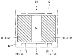
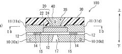
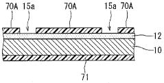
- A method involving the formation of a semiconductor structure on a metal foil, covering it with a resin film, and using laser irradiation to create openings and heat-treat the semiconductor surface, improving film quality and TFT characteristics.
Flexible semiconductor device and manufacturing method therefor
PatentWO2011142081A1
Innovation
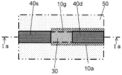
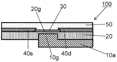
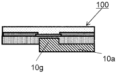
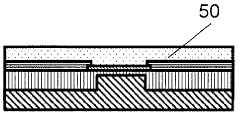
- A flexible semiconductor device with a structure featuring semiconductor elements on a resin substrate, where the insulating film has varying thicknesses to minimize parasitic capacitance, and the gate electrode protrudes to reduce capacitance between wiring layers, using metal foils for support and high-temperature semiconductor materials.
Manufacturing Process Optimization for Flexible Displays
Manufacturing process optimization for flexible displays represents a critical frontier in advancing the performance capabilities of semiconductor-based flexible display technologies. The transition from rigid to flexible substrates necessitates fundamental reconsideration of traditional manufacturing approaches to accommodate the unique properties of flexible materials while maintaining or enhancing semiconductor performance.
Low-temperature processing techniques have emerged as essential innovations in flexible display manufacturing. Unlike conventional silicon-based displays requiring high-temperature processing (>300°C), flexible substrates such as polyimide and PET demand processing temperatures below 200°C to prevent substrate deformation. Advanced techniques including low-temperature poly-silicon (LTPS) and oxide semiconductor deposition have been developed specifically to address this constraint while maintaining semiconductor quality.
Roll-to-roll (R2R) processing represents another significant manufacturing advancement, enabling continuous production of flexible displays on polymer substrates. This approach dramatically increases throughput compared to traditional batch processing methods. Recent innovations in R2R systems have achieved web handling precision below 5μm, critical for maintaining registration accuracy across multiple deposition and patterning steps in semiconductor layer formation.
Thin-film encapsulation (TFE) technologies have revolutionized barrier layer formation for flexible displays. Multi-layer organic-inorganic structures created through atomic layer deposition (ALD) achieve water vapor transmission rates below 10^-6 g/m²/day, protecting sensitive semiconductor materials from environmental degradation while maintaining flexibility. These encapsulation techniques have reduced layer thickness by over 70% compared to first-generation technologies.
Laser processing has supplanted conventional photolithography in many flexible display manufacturing steps. Direct laser patterning enables precise semiconductor feature definition without subjecting flexible substrates to harsh chemical processes. Recent developments in ultrafast lasers have achieved feature sizes below 2μm with minimal heat-affected zones, preserving both substrate integrity and semiconductor performance characteristics.
Stress management techniques represent perhaps the most critical manufacturing optimization area. Neutral plane engineering, where semiconductor layers are positioned at the mechanical neutral plane of the structure, has demonstrated up to 85% reduction in strain-induced performance degradation during bending. Complementary approaches including strain-isolation layers and geometric patterning (such as serpentine interconnects) further enhance semiconductor reliability under mechanical deformation.
Durability and Reliability Assessment Methods
Assessing the durability and reliability of flexible display substrates requires comprehensive methodologies that address their unique characteristics and performance requirements. Traditional rigid substrate testing protocols are insufficient for evaluating flexible materials that must withstand repeated bending, folding, and environmental stresses while maintaining semiconductor performance.
Accelerated aging tests represent a cornerstone of reliability assessment for flexible substrates. These tests subject materials to intensified environmental conditions—including elevated temperatures (typically 60-85°C), high humidity (85-95%), and UV exposure—to simulate years of usage within weeks. The semiconductor performance parameters are measured before and after exposure to quantify degradation rates and establish lifetime predictions.
Mechanical endurance testing employs specialized equipment that performs cyclic bending, folding, and rolling operations. Advanced systems can execute up to 200,000 cycles while simultaneously monitoring electrical performance parameters. The industry standard typically requires flexible displays to maintain functionality after a minimum of 100,000 bending cycles at radii between 1-5mm, depending on the application requirements.
Environmental resistance evaluation examines how flexible substrates and their semiconductor components respond to temperature fluctuations (-40°C to 85°C), humidity variations, and chemical exposure. Thermal cycling tests are particularly critical as the different thermal expansion coefficients between substrate layers and semiconductor materials can induce stress that compromises performance over time.
Impact and drop testing protocols have been adapted specifically for flexible displays, focusing on both the substrate integrity and the continued functionality of semiconductor components. These tests typically involve drops from standardized heights (0.8-1.5m) onto various surfaces while monitoring for changes in electrical characteristics and physical damage.
Non-destructive evaluation techniques provide crucial insights without compromising sample integrity. These include optical coherence tomography, infrared thermography, and acoustic microscopy to detect delamination, microcracks, and other defects that may affect semiconductor performance. Real-time monitoring systems can track changes during mechanical stress application, offering valuable data on failure mechanisms.
Electrical performance stability under mechanical stress represents perhaps the most critical assessment metric. This involves measuring key semiconductor parameters—carrier mobility, threshold voltage, leakage current, and on/off ratios—while the substrate undergoes controlled deformation. Advanced testing platforms can simultaneously apply mechanical stress while performing electrical characterization, providing direct correlation between physical deformation and performance degradation.
Unlock deeper insights with PatSnap Eureka Quick Research — get a full tech report to explore trends and direct your research. Try now!
Generate Your Research Report Instantly with AI Agent
Supercharge your innovation with PatSnap Eureka AI Agent Platform!
