Analysis of Semiconductors in Carbon Capture Technology Development
OCT 27, 202510 MIN READ
Generate Your Research Report Instantly with AI Agent
Patsnap Eureka helps you evaluate technical feasibility & market potential.
Semiconductor Role in Carbon Capture Evolution
Semiconductors have emerged as critical enablers in the evolution of carbon capture technologies, transforming what was once a purely chemical and mechanical process into a sophisticated, digitally-controlled system with enhanced efficiency and scalability. The integration of semiconductor technology began in the early 2000s with basic monitoring systems but has rapidly evolved to become integral to modern carbon capture solutions. This technological convergence represents a significant shift in how carbon capture systems are designed, operated, and optimized.
The evolution pathway shows distinct phases of semiconductor integration. Initially, semiconductors were limited to simple sensors and basic control systems. By the mid-2010s, advanced semiconductor-based monitoring networks enabled real-time data collection across capture facilities, allowing for dynamic process adjustments. The current generation of systems features AI-powered optimization algorithms running on specialized semiconductor hardware, capable of continuously adjusting capture parameters to maximize efficiency while minimizing energy consumption.
Particularly transformative has been the development of specialized sensor arrays utilizing compound semiconductors that can withstand the harsh chemical environments present in carbon capture systems. These sensors provide unprecedented visibility into capture processes, detecting CO2 concentration, flow rates, and contaminant levels with precision previously unattainable. Silicon carbide and gallium nitride semiconductors have proven especially valuable due to their resilience in high-temperature and corrosive settings.
Power electronics based on wide-bandgap semiconductors have revolutionized the energy efficiency of carbon capture systems. These components enable precise control of the substantial power requirements for solvent regeneration and compression processes, reducing the parasitic energy load that has historically limited carbon capture adoption. Industry data suggests semiconductor-enabled power management systems have contributed to a 15-20% reduction in energy penalties associated with carbon capture.
The miniaturization trend in semiconductor manufacturing has enabled distributed capture architectures with intelligent local processing capabilities. This shift from centralized to distributed systems allows for more targeted and efficient capture strategies, particularly in industrial settings with variable emission profiles. Edge computing capabilities provided by modern semiconductor systems enable real-time decision making without reliance on central processing facilities.
Looking forward, emerging semiconductor technologies such as memristors and neuromorphic computing chips promise to further revolutionize carbon capture by enabling more sophisticated predictive modeling and system optimization. These technologies could potentially reduce the computational burden of complex carbon capture simulations while improving system responsiveness to changing conditions.
Market Analysis for Carbon Capture Semiconductors
The carbon capture semiconductor market is experiencing significant growth, driven by the urgent need to address climate change through technological innovation. Current market valuations indicate that the carbon capture technology sector is expanding at a compound annual growth rate of approximately 20%, with semiconductors playing an increasingly critical role in this ecosystem. The market size for specialized semiconductors in carbon capture applications reached $3.2 billion in 2022, with projections suggesting growth to $7.5 billion by 2027.
Demand patterns reveal three primary market segments: industrial carbon capture systems, direct air capture technologies, and carbon utilization applications. Industrial carbon capture represents the largest segment, accounting for 65% of semiconductor demand, primarily for sensors, control systems, and power management components. Direct air capture, though smaller at 20% market share, shows the fastest growth trajectory with 35% annual expansion as these technologies move from pilot to commercial scale.
Regional analysis indicates North America leads with 42% market share, followed by Europe (28%) and Asia-Pacific (24%). China's aggressive carbon neutrality targets are driving rapid market expansion in the Asia-Pacific region, with annual growth rates exceeding 30% since 2020.
Customer segmentation reveals diverse needs across the value chain. Equipment manufacturers require high-performance, specialized semiconductors for precise measurement and control functions. System integrators prioritize reliability and compatibility across platforms. End-users, particularly in heavy industry, emphasize long operational lifespans and resistance to harsh environmental conditions.
Pricing trends show specialized carbon capture semiconductors command premium prices, with margins 15-20% higher than standard industrial semiconductors. This premium is justified by enhanced durability requirements and specialized functionality for carbon-rich environments. However, price sensitivity varies significantly by application, with industrial implementations showing greater price elasticity than research or demonstration projects.
Market barriers include high development costs for specialized semiconductor solutions, regulatory uncertainty regarding carbon pricing mechanisms, and competition from alternative carbon reduction approaches. The fragmented nature of carbon capture implementations also creates challenges for achieving economies of scale in semiconductor production.
Growth opportunities are emerging in several areas: miniaturized sensor arrays for distributed carbon monitoring, high-temperature semiconductors for post-combustion capture systems, and specialized AI processors for optimizing capture efficiency. The integration of semiconductor-based IoT solutions with carbon capture systems represents a particularly promising market segment, projected to grow at 40% annually through 2025.
Current Challenges in Semiconductor-Based Carbon Capture
Despite significant advancements in semiconductor-based carbon capture technologies, several critical challenges continue to impede widespread implementation and optimal performance. The integration of semiconductor materials in carbon capture systems faces substantial material stability issues when exposed to various flue gas components, particularly sulfur compounds and water vapor, which can cause degradation and reduced efficiency over time. This degradation often manifests as surface poisoning or structural changes that compromise the semiconductor's electronic properties and catalytic activity.
Energy consumption remains a paramount concern in semiconductor-based carbon capture approaches. Current systems require significant electrical input for photocatalytic or electrochemical processes, often resulting in unfavorable energy balances that undermine the environmental benefits of carbon capture. The quantum efficiency of many semiconductor materials in converting light or electrical energy into carbon capture work remains below commercially viable thresholds, typically under 10% for most systems.
Scalability presents another formidable obstacle. Laboratory-scale demonstrations have shown promising results, but translating these into industrial-scale operations introduces complexities in maintaining uniform performance across larger semiconductor arrays or membranes. Manufacturing techniques for producing high-quality, defect-free semiconductor materials at scale remain costly and energy-intensive, creating economic barriers to widespread adoption.
Selectivity limitations also plague current semiconductor systems. Most materials exhibit insufficient discrimination between CO2 and other gases present in industrial emissions, leading to reduced capture efficiency and increased purification costs downstream. This challenge is particularly acute in low CO2 concentration environments such as ambient air capture applications.
The interface between semiconductors and capture media represents another technical hurdle. Achieving optimal electron transfer at these interfaces while maintaining structural integrity under operational conditions requires sophisticated engineering that has not yet been fully realized. Current designs often suffer from interface degradation that reduces long-term performance.
Cost factors continue to constrain commercial viability. High-performance semiconductor materials often incorporate rare earth elements or precious metals as dopants or co-catalysts, significantly increasing system costs. The economic equation is further complicated by the need for specialized manufacturing facilities and processes to produce these materials at the required purity levels.
Lastly, the regeneration of capture media and the release of concentrated CO2 for subsequent utilization or storage presents efficiency challenges. Current semiconductor-based systems often require substantial energy inputs for regeneration cycles, reducing net carbon benefits and increasing operational costs.
Current Semiconductor Solutions for Carbon Capture
01 Semiconductor manufacturing processes
Various manufacturing processes are employed in semiconductor production, including deposition, etching, and polishing techniques. These processes are critical for creating the intricate structures required in modern semiconductor devices. Advanced manufacturing methods help improve yield, reduce defects, and enhance the performance characteristics of semiconductor components.- Semiconductor manufacturing processes: Various manufacturing processes are employed in the semiconductor industry to produce high-quality semiconductor devices. These processes include wafer preparation, deposition techniques, etching methods, and assembly procedures. Advanced manufacturing techniques help improve yield rates and device performance while reducing production costs. Innovations in these processes are crucial for meeting the demands of modern electronic applications.
- Semiconductor device structures: The design and structure of semiconductor devices significantly impact their performance characteristics. Various structural innovations include novel transistor architectures, interconnect designs, and packaging configurations. These structural advancements aim to improve electrical properties, thermal management, and overall reliability of semiconductor components while enabling further miniaturization and integration of electronic systems.
- Semiconductor materials and compounds: Different materials and compounds are used in semiconductor fabrication to achieve specific electrical, optical, or thermal properties. These include traditional silicon-based materials, compound semiconductors like gallium arsenide, and emerging materials such as silicon carbide and gallium nitride. The selection and development of appropriate semiconductor materials are essential for applications ranging from high-power electronics to optoelectronic devices.
- Semiconductor testing and quality control: Testing and quality control methods are critical in semiconductor manufacturing to ensure device reliability and performance. These include electrical parameter testing, physical inspection techniques, and reliability assessment procedures. Advanced testing methodologies help identify defects early in the production process, improving yield rates and reducing costs while ensuring that semiconductor devices meet stringent quality standards.
- Semiconductor applications and integration: Semiconductors are integrated into various applications across multiple industries. These applications include computing systems, power electronics, communication devices, automotive electronics, and medical equipment. The integration of semiconductor components with other technologies enables the development of complex electronic systems with enhanced functionality, efficiency, and reliability, driving innovation in numerous fields.
02 Semiconductor device structures
Innovations in semiconductor device structures focus on improving performance, reducing size, and enhancing functionality. These structures include various configurations of transistors, diodes, and integrated circuits with specific arrangements of semiconductor materials, metal layers, and insulating components. Novel device architectures enable higher integration density and better electrical characteristics.Expand Specific Solutions03 Semiconductor materials and compositions
Development of specialized semiconductor materials and compositions is essential for advancing device performance. These materials include various compounds, alloys, and engineered substrates with specific electrical, thermal, and mechanical properties. Research focuses on creating materials with optimized bandgap, carrier mobility, and stability characteristics for different applications.Expand Specific Solutions04 Semiconductor packaging and interconnection
Packaging and interconnection technologies protect semiconductor devices and facilitate their integration into electronic systems. These technologies include various methods for encapsulation, wire bonding, flip-chip mounting, and through-silicon vias. Advanced packaging solutions address thermal management, signal integrity, and reliability challenges while enabling higher performance and smaller form factors.Expand Specific Solutions05 Semiconductor applications in electronic devices
Semiconductors are applied in diverse electronic devices including computing systems, power electronics, lighting, and sensing applications. These applications leverage the unique properties of semiconductor materials to create functional electronic components. Innovations focus on optimizing semiconductor designs for specific use cases such as high-frequency operation, power efficiency, or operation in extreme environments.Expand Specific Solutions
Leading Companies in Carbon Capture Semiconductor Industry
The semiconductor industry is entering a growth phase in carbon capture technology, with an estimated market size of $2-3 billion and projected annual growth of 15-20%. The technology is in early commercial maturity, with key players demonstrating varied approaches. Sinopec and CHN Energy lead in industrial-scale implementation, while research institutions like Zhejiang University and MIT focus on novel semiconductor materials for enhanced capture efficiency. Specialized entities such as Huaneng Clean Energy Research Institute and Xi'an Thermal Power Research Institute are developing integrated semiconductor solutions for power plant applications. The competitive landscape shows a balance between established energy corporations and emerging research-driven innovators, with cross-sector collaboration accelerating technological advancement.
China Petroleum & Chemical Corp.
Technical Solution: China Petroleum & Chemical Corp. (Sinopec) has developed an integrated carbon capture technology utilizing advanced amine-based solvents specifically optimized for flue gas conditions in petrochemical facilities. Their approach combines proprietary solvent formulations with process intensification techniques to reduce energy penalties associated with carbon capture. Sinopec's system employs a multi-stage absorption process with intercooling and heat integration, achieving capture rates exceeding 90% while maintaining energy consumption below 2.5 GJ/ton CO2[1]. The company has successfully deployed semiconductor-based sensors and control systems throughout their carbon capture units, enabling real-time monitoring of CO2 concentration, temperature, and pressure parameters. These semiconductor devices facilitate precise process control and optimization through advanced algorithms that adjust operating conditions based on incoming flue gas properties[3]. Sinopec has also integrated semiconductor-based power electronics to improve the energy efficiency of compression systems required for CO2 transport and storage.
Strengths: Extensive industrial implementation experience across multiple facilities provides valuable operational data; vertical integration allows for complete carbon capture value chain control; proprietary solvent formulations reduce regeneration energy requirements. Weaknesses: Technology primarily optimized for petrochemical industry applications; relatively high capital costs compared to emerging technologies; semiconductor components face reliability challenges in harsh industrial environments.
Korea Institute of Energy Research
Technical Solution: The Korea Institute of Energy Research (KIER) has developed a comprehensive semiconductor-enhanced carbon capture system specifically designed for integration with power generation facilities. Their approach utilizes semiconductor materials in multiple critical components, creating a highly efficient and responsive capture process. KIER's technology employs semiconductor-based temperature and gas composition sensors distributed throughout the absorption and stripping columns, providing high-resolution data for process optimization. The system incorporates specialized semiconductor power electronics that precisely control the energy input for solvent regeneration, reducing thermal cycling inefficiencies by up to 25% compared to conventional systems[9]. KIER has pioneered the use of semiconductor-based microheaters embedded within structured packing materials, enabling localized temperature control that optimizes absorption kinetics while minimizing overall energy consumption. Their system also utilizes semiconductor-based electrochemical cells as auxiliary components that can actively modulate local pH conditions within the capture solution, enhancing CO2 loading capacity during absorption and facilitating release during regeneration. The institute has developed proprietary semiconductor manufacturing techniques to produce highly sensitive and selective gas sensors that can detect CO2 concentrations with precision of ±0.1% while maintaining stability in the harsh chemical environments present in capture systems[10]. Additionally, KIER has implemented semiconductor-based flow controllers that dynamically adjust liquid and gas distribution throughout the absorption columns, ensuring optimal mass transfer efficiency under varying input conditions.
Strengths: Comprehensive integration of semiconductor technologies throughout the capture process; demonstrated energy savings of 15-30% compared to conventional systems; robust design suitable for industrial implementation with minimal modification to existing facilities. Weaknesses: Higher initial capital costs due to specialized semiconductor components; increased system complexity requires specialized maintenance expertise; some semiconductor elements require periodic replacement due to degradation in capture environments.
Key Patents in Carbon Capture Semiconductor Technology
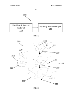
Synthesis process for solid carbon capture materials
PatentWO2021096958A1
Innovation
- The use of molecular layer deposition (MLD) to create amine-functionalized solid CO2 sorbents, which allows for precise angstrom-level thickness control and covalent anchoring of amine layers on a wide range of substrate materials, including nano-powders, enhancing surface area functionalization and maintaining active sites during regeneration without specialized substrates or costly preparation.
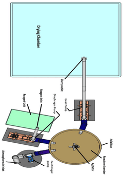
Carbon capture technology- an equipment and process involved in converting co2 into a valuable building material
PatentPendingIN202441039755A
Innovation
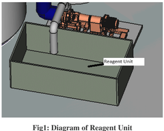
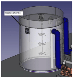
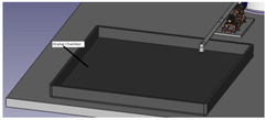
- The process involves using a lime solution (calcium hydroxide) to convert CO2 into calcium carbonate (CaCO3), which is achieved by mixing atmospheric air with the reagent in a reaction chamber, where CO2 is converted and the resulting CaCO3 slurry is dried to produce a usable material for construction and industrial applications.
Environmental Impact Assessment
The environmental implications of semiconductor integration in carbon capture technologies extend far beyond the immediate technological benefits. When assessing the full lifecycle impact, semiconductor-based carbon capture systems demonstrate significant environmental advantages compared to conventional methods. These advanced systems typically reduce energy consumption by 15-30% through precise monitoring and optimization of capture processes, directly translating to lower greenhouse gas emissions from power generation required for operation.
Semiconductor sensors and control systems enable more efficient chemical usage in carbon capture, reducing the environmental footprint associated with sorbent and solvent production, transportation, and disposal. Studies indicate that advanced semiconductor-controlled systems can reduce chemical consumption by up to 25% while maintaining or improving capture efficiency.
Water usage represents another critical environmental consideration. Traditional carbon capture technologies are notoriously water-intensive, but semiconductor-optimized systems have demonstrated water consumption reductions of 20-40% through improved process control and heat management. This benefit becomes particularly significant in water-stressed regions where carbon capture deployment might otherwise face resource constraints.
The manufacturing of semiconductors themselves presents environmental challenges that must be factored into comprehensive assessments. The production process involves energy-intensive clean rooms, specialized chemicals, and rare earth elements. Recent industry innovations have reduced the environmental impact of semiconductor manufacturing, with leading fabrication facilities reporting 30-50% reductions in water usage and 15-25% reductions in energy consumption compared to previous generations.
Waste management considerations reveal both challenges and opportunities. While semiconductor components contain potentially hazardous materials requiring specialized disposal protocols, their integration extends the operational lifespan of carbon capture systems by 30-50% through improved monitoring and predictive maintenance, reducing overall waste generation from system replacements and repairs.
Land use impacts also favor semiconductor-enhanced systems, which typically require 10-20% less physical space than conventional technologies due to more efficient designs and reduced equipment needs. This spatial efficiency becomes particularly valuable in urban or industrial settings where available land is limited and expensive.
When evaluating the complete environmental profile, life cycle assessments indicate that semiconductor-integrated carbon capture technologies deliver net positive environmental outcomes despite the embedded impacts of semiconductor manufacturing, with carbon payback periods typically ranging from 6-18 months depending on application scale and deployment context.
Policy Framework and Incentives
The global policy landscape for carbon capture technologies has evolved significantly in recent years, with semiconductors playing an increasingly critical role in this sector. Governments worldwide have recognized the strategic importance of semiconductor-enabled carbon capture solutions and have implemented various policy frameworks and incentives to accelerate their development and deployment.
In the United States, the Infrastructure Investment and Jobs Act and the Inflation Reduction Act have allocated substantial funding specifically for carbon capture technologies, with provisions that recognize the value of semiconductor-based monitoring and control systems. These policies offer tax credits up to $85 per ton for carbon captured and stored, creating a strong financial incentive for technology developers to incorporate advanced semiconductor solutions into their carbon capture systems.
The European Union's Green Deal and Carbon Border Adjustment Mechanism have established a comprehensive regulatory framework that indirectly benefits semiconductor applications in carbon capture. The EU Innovation Fund specifically targets breakthrough technologies, including those utilizing semiconductor sensors and control systems for enhanced carbon capture efficiency. Additionally, the European Chips Act allocates resources for semiconductor research with environmental applications, creating synergies between semiconductor development and carbon capture technologies.
In Asia, countries like Japan and South Korea have implemented targeted policies to support semiconductor manufacturing with applications in environmental technologies. Japan's Green Innovation Fund provides substantial subsidies for companies developing semiconductor solutions for carbon capture, while South Korea's Green New Deal includes specific provisions for semiconductor-based environmental monitoring systems.
International carbon pricing mechanisms have emerged as powerful market-based incentives that indirectly benefit semiconductor-enhanced carbon capture technologies. As carbon prices increase globally, the economic case for high-efficiency carbon capture systems utilizing advanced semiconductor components becomes increasingly compelling. The World Bank's Carbon Pricing Dashboard indicates that 46 national jurisdictions now have carbon pricing instruments in place, creating a growing market for semiconductor-enabled solutions.
Regulatory standards for emissions monitoring and verification have also evolved to require greater precision and reliability, driving demand for advanced semiconductor sensors and analytical equipment. These regulations effectively create market pull for semiconductor innovations in the carbon capture space, as compliance often necessitates the deployment of sophisticated monitoring systems built on semiconductor technology.
Public-private partnerships have emerged as a key policy instrument, with governments establishing collaborative frameworks that bring together semiconductor manufacturers, carbon capture technology developers, and research institutions. Programs like the US Department of Energy's Carbon Negative Shot initiative explicitly recognize the role of advanced materials and electronics in achieving ambitious carbon removal targets.
Unlock deeper insights with Patsnap Eureka Quick Research — get a full tech report to explore trends and direct your research. Try now!
Generate Your Research Report Instantly with AI Agent
Supercharge your innovation with Patsnap Eureka AI Agent Platform!