Analysis of Semiconductors in Nitrogen Reduction Catalyst Design
SEP 28, 20259 MIN READ
Generate Your Research Report Instantly with AI Agent
Patsnap Eureka helps you evaluate technical feasibility & market potential.
Semiconductor Catalysis Background and Objectives
Semiconductor materials have emerged as pivotal components in the development of efficient nitrogen reduction catalysts, marking a significant evolution in ammonia synthesis technology. The traditional Haber-Bosch process, while industrially dominant for over a century, operates under harsh conditions requiring temperatures of 400-500°C and pressures of 150-300 bar, consuming approximately 1-2% of global energy production. This energy-intensive process has driven researchers to explore alternative approaches, with semiconductor-based catalysts representing one of the most promising directions.
The historical trajectory of semiconductor catalysis for nitrogen reduction began in the 1970s with preliminary investigations into photocatalytic processes. However, significant breakthroughs only materialized in the early 2000s when researchers demonstrated the feasibility of using semiconductor materials to activate the exceptionally stable N≡N triple bond under ambient conditions. This progress has accelerated dramatically in the past decade, with publications in this field increasing by approximately 300% between 2010 and 2020.
Current technological objectives in semiconductor-based nitrogen reduction catalysis center on three primary goals: enhancing catalytic efficiency, improving selectivity toward ammonia production, and developing systems capable of operating under ambient conditions. The benchmark target established by researchers is to achieve a Faradaic efficiency exceeding 60% with an ammonia production rate greater than 10^-9 mol cm^-2 s^-1, parameters that would position this technology as commercially viable.
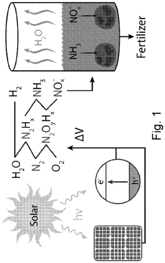
The fundamental principles underlying semiconductor catalysis for nitrogen reduction involve the generation of electron-hole pairs through light absorption or electrical stimulation. These charge carriers can then participate in redox reactions at the catalyst surface, facilitating the breaking of the N≡N bond and subsequent protonation steps. Various semiconductor materials including TiO2, ZnO, g-C3N4, and more recently, 2D materials such as MXenes and transition metal dichalcogenides, have demonstrated promising capabilities in this regard.
The technological evolution in this field is trending toward hybrid systems that combine semiconductors with co-catalysts, plasmonic materials, or defect engineering strategies to overcome inherent limitations in charge separation and surface reactivity. Computational studies using density functional theory have become instrumental in predicting optimal semiconductor compositions and surface structures for nitrogen activation.
Looking forward, the trajectory of semiconductor catalysis in nitrogen reduction is expected to converge with advances in renewable energy integration, enabling sustainable ammonia production systems powered by solar or wind energy. This alignment with green energy sources represents the ultimate objective: developing a carbon-neutral alternative to the Haber-Bosch process that can address both agricultural fertilizer needs and emerging applications in hydrogen storage and fuel cells.
The historical trajectory of semiconductor catalysis for nitrogen reduction began in the 1970s with preliminary investigations into photocatalytic processes. However, significant breakthroughs only materialized in the early 2000s when researchers demonstrated the feasibility of using semiconductor materials to activate the exceptionally stable N≡N triple bond under ambient conditions. This progress has accelerated dramatically in the past decade, with publications in this field increasing by approximately 300% between 2010 and 2020.
Current technological objectives in semiconductor-based nitrogen reduction catalysis center on three primary goals: enhancing catalytic efficiency, improving selectivity toward ammonia production, and developing systems capable of operating under ambient conditions. The benchmark target established by researchers is to achieve a Faradaic efficiency exceeding 60% with an ammonia production rate greater than 10^-9 mol cm^-2 s^-1, parameters that would position this technology as commercially viable.
The fundamental principles underlying semiconductor catalysis for nitrogen reduction involve the generation of electron-hole pairs through light absorption or electrical stimulation. These charge carriers can then participate in redox reactions at the catalyst surface, facilitating the breaking of the N≡N bond and subsequent protonation steps. Various semiconductor materials including TiO2, ZnO, g-C3N4, and more recently, 2D materials such as MXenes and transition metal dichalcogenides, have demonstrated promising capabilities in this regard.
The technological evolution in this field is trending toward hybrid systems that combine semiconductors with co-catalysts, plasmonic materials, or defect engineering strategies to overcome inherent limitations in charge separation and surface reactivity. Computational studies using density functional theory have become instrumental in predicting optimal semiconductor compositions and surface structures for nitrogen activation.
Looking forward, the trajectory of semiconductor catalysis in nitrogen reduction is expected to converge with advances in renewable energy integration, enabling sustainable ammonia production systems powered by solar or wind energy. This alignment with green energy sources represents the ultimate objective: developing a carbon-neutral alternative to the Haber-Bosch process that can address both agricultural fertilizer needs and emerging applications in hydrogen storage and fuel cells.
Market Analysis for Nitrogen Fixation Technologies
The global nitrogen fixation technologies market is experiencing significant growth, driven by increasing demand for fertilizers in agriculture and various industrial applications. Currently valued at approximately 25 billion USD, this market is projected to grow at a compound annual growth rate of 3.7% through 2030, with the semiconductor-based catalytic nitrogen reduction segment emerging as one of the fastest-growing sectors.
Agricultural applications dominate the market, accounting for nearly 70% of the total demand, as nitrogen-based fertilizers remain essential for global food security. Industrial applications, including chemical manufacturing and pharmaceuticals, constitute the remaining 30%, with steady growth observed in specialized nitrogen compounds for advanced materials.
Regionally, Asia-Pacific leads the market with over 45% share, primarily due to extensive agricultural activities in China and India, coupled with rapid industrialization. North America and Europe follow with approximately 25% and 20% market shares respectively, where the focus is increasingly shifting toward sustainable nitrogen fixation technologies, particularly semiconductor-based catalytic systems that offer improved efficiency and reduced environmental impact.
The traditional Haber-Bosch process continues to dominate commercial nitrogen fixation, representing over 80% of global production capacity. However, this segment is growing at a modest 2% annually, while emerging technologies, especially semiconductor-based electrochemical and photocatalytic nitrogen reduction approaches, are experiencing growth rates exceeding 15% annually, albeit from a smaller base.
Market dynamics are increasingly influenced by sustainability concerns and regulatory pressures. Countries implementing stricter environmental regulations are creating premium markets for low-carbon nitrogen fixation technologies. The European Green Deal and similar initiatives in North America are accelerating the adoption of semiconductor-based catalysts that can operate at ambient conditions with renewable energy inputs.
Investment trends reveal growing venture capital interest in startups developing semiconductor-based nitrogen reduction catalysts, with funding increasing from 120 million USD in 2018 to over 450 million USD in 2022. Major agricultural input companies and chemical manufacturers are also establishing strategic partnerships with technology developers, recognizing the potential for disruption in traditional nitrogen production methods.
Consumer markets are showing increased willingness to pay premium prices for products manufactured using sustainable nitrogen fixation technologies, creating additional market pull for semiconductor-based solutions. This trend is particularly evident in organic farming, specialty chemicals, and pharmaceutical manufacturing sectors where environmental footprint is becoming a key purchasing consideration.
Current Challenges in Semiconductor-Based Nitrogen Reduction
Despite significant advancements in semiconductor-based nitrogen reduction catalysts, several critical challenges continue to impede widespread implementation and commercialization. The fundamental challenge remains the strong triple bond (941 kJ/mol) in N₂ molecules, which requires substantial energy input for activation. Semiconductor materials, while promising for their tunable electronic properties, still struggle with achieving activation energies low enough for practical applications under ambient conditions.
Selectivity presents another major obstacle, as competing reactions—particularly hydrogen evolution—often dominate in aqueous environments. Current semiconductor catalysts typically demonstrate N₂ reduction reaction (NRR) Faradaic efficiencies below 15%, with many reporting single-digit percentages. This poor selectivity significantly hampers ammonia production rates and energy efficiency.
Stability issues plague semiconductor catalysts under NRR conditions. Surface oxidation, photocorrosion, and structural degradation frequently occur during extended operation periods. For instance, metal oxide semiconductors often suffer from dissolution in acidic electrolytes, while metal sulfides may undergo surface oxidation that alters their catalytic properties.
The identification and quantification of produced ammonia remains problematic, with potential contamination from atmospheric nitrogen compounds leading to false positives. Current detection methods like the indophenol blue method and ion chromatography have detection limits that challenge accurate measurement of the typically low ammonia yields from semiconductor-based systems.
Scalability represents a significant engineering challenge. Laboratory-scale demonstrations often utilize expensive materials and controlled conditions that prove difficult to translate to industrial settings. The synthesis of uniform, defect-controlled semiconductor catalysts at scale remains technically demanding and cost-prohibitive.
Energy efficiency metrics for semiconductor-based NRR systems remain disappointingly low. Current systems typically require energy inputs exceeding 100 MWh per ton of ammonia produced, far higher than the conventional Haber-Bosch process (approximately 10 MWh/ton). This energy gap must be narrowed substantially for these technologies to become economically viable alternatives.
Interface engineering between semiconductors and electrolytes presents complex challenges in charge transfer dynamics. The semiconductor-electrolyte interface often suffers from rapid charge recombination, limiting the availability of energetic electrons for N₂ reduction. Additionally, the mechanistic understanding of reaction pathways on semiconductor surfaces remains incomplete, hampering rational catalyst design approaches.
Current Semiconductor Catalyst Design Approaches
01 Semiconductor-based catalysts for nitrogen reduction
Semiconductor materials can be utilized as catalysts or catalyst supports for nitrogen reduction reactions. These materials offer unique electronic properties that can enhance electron transfer during the catalytic process. The band gap structure of semiconductors can be tuned to optimize the nitrogen reduction efficiency. Various semiconductor materials including metal oxides, nitrides, and composite structures have shown promising results in nitrogen fixation applications.- Semiconductor-based catalysts for nitrogen reduction: Semiconductor materials can be used as catalysts for nitrogen reduction reactions. These materials provide unique electronic properties that facilitate electron transfer during the reduction process. By engineering the band gap and surface properties of semiconductors, the efficiency of nitrogen reduction can be significantly improved. Various semiconductor materials including metal oxides, nitrides, and composite structures have shown promising catalytic activity for converting nitrogen to ammonia under mild conditions.
- Metal-semiconductor hybrid catalysts: Hybrid catalysts combining metals with semiconductors create synergistic effects that enhance nitrogen reduction efficiency. The metal components often serve as active sites for nitrogen adsorption and activation, while the semiconductor provides efficient electron transfer pathways. These hybrid structures can overcome limitations of traditional catalysts by optimizing both adsorption energy and electron availability. The interface between metal and semiconductor plays a crucial role in determining the overall catalytic performance for nitrogen reduction reactions.
- Nanostructured semiconductor catalysts for improved efficiency: Nanostructuring of semiconductor catalysts significantly enhances nitrogen reduction efficiency by increasing the surface area and creating more active sites. Various nanostructures including nanoparticles, nanowires, nanosheets, and porous architectures have been developed to maximize catalytic performance. These nanostructured semiconductors often exhibit quantum confinement effects that can be tuned to optimize the electronic properties for nitrogen reduction. Additionally, the high surface-to-volume ratio of nanostructured catalysts allows for better utilization of catalyst material and improved mass transfer during the reaction.
- Doped semiconductor catalysts for nitrogen reduction: Doping semiconductors with various elements can significantly enhance their catalytic activity for nitrogen reduction. Dopants modify the electronic structure of the semiconductor, creating defect sites that can serve as active centers for nitrogen adsorption and activation. Common dopants include transition metals, non-metals, and rare earth elements. The type and concentration of dopants can be optimized to achieve the desired electronic properties and catalytic performance. Doped semiconductor catalysts often show improved selectivity and lower overpotential for nitrogen reduction reactions.
- Photocatalytic semiconductor systems for nitrogen reduction: Photocatalytic semiconductor systems utilize light energy to drive nitrogen reduction reactions under ambient conditions. These systems typically consist of semiconductor materials with appropriate band gaps that can absorb visible or UV light to generate electron-hole pairs. The photogenerated electrons are then used to reduce nitrogen molecules. Various strategies including heterojunction formation, cocatalyst loading, and surface modification have been employed to enhance the efficiency of photocatalytic nitrogen reduction. These systems offer the advantage of operating under mild conditions using renewable solar energy.
02 Metal-semiconductor hybrid catalysts
Hybrid catalysts combining metals with semiconductor materials demonstrate enhanced efficiency in nitrogen reduction reactions. The metal components often serve as active sites for nitrogen adsorption and activation, while the semiconductor provides electronic support and modifies the electronic structure of the metal. These synergistic effects can significantly improve catalyst performance by facilitating electron transfer and optimizing binding energies for reaction intermediates.Expand Specific Solutions03 Nanostructured catalysts for improved efficiency
Nanostructuring of semiconductor catalysts can dramatically enhance nitrogen reduction efficiency by increasing the surface area and exposing more active sites. Various nanostructures including nanoparticles, nanowires, nanosheets, and porous architectures have been developed to maximize catalytic performance. The controlled synthesis of these nanostructures allows for precise engineering of catalyst properties, resulting in improved nitrogen activation and conversion rates.Expand Specific Solutions04 Doping strategies to enhance semiconductor catalyst activity
Doping semiconductor materials with various elements can significantly enhance their catalytic activity for nitrogen reduction. Dopants can modify the electronic structure, create oxygen vacancies, or introduce defect sites that serve as active centers for nitrogen adsorption and activation. Strategic doping can optimize the binding energy of reaction intermediates and lower the activation energy barrier, resulting in improved catalytic efficiency and selectivity.Expand Specific Solutions05 Reactor design and process optimization for semiconductor catalysts
The efficiency of semiconductor-based nitrogen reduction catalysts is heavily influenced by reactor design and process conditions. Factors such as temperature, pressure, gas flow rates, and reactor configuration can significantly impact catalyst performance. Advanced reactor designs that optimize mass transfer, heat management, and light utilization (for photocatalysts) have been developed to maximize the efficiency of semiconductor catalysts in practical nitrogen fixation applications.Expand Specific Solutions
Leading Organizations in Semiconductor Catalyst Research
The semiconductor industry in nitrogen reduction catalyst design is currently in an early growth phase, characterized by significant research activity but limited commercial deployment. The market size is expanding rapidly, driven by increasing demand for sustainable ammonia production technologies, with projections suggesting a multi-billion dollar opportunity by 2030. Technologically, the field remains in development with varying levels of maturity across players. Academic institutions like Zhejiang University, Tianjin University, and Georgia Tech Research Corp. are advancing fundamental research, while companies including Topsoe A/S and Johnson Matthey demonstrate more mature catalyst technologies. Semiconductor manufacturers such as GLOBALFOUNDRIES, Macronix, and Sanken Electric are exploring integration opportunities, leveraging their expertise in materials science and nanofabrication to enhance catalyst performance and scalability.
Tianjin University
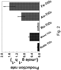
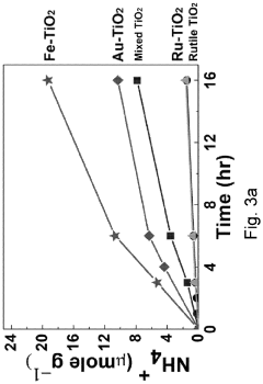
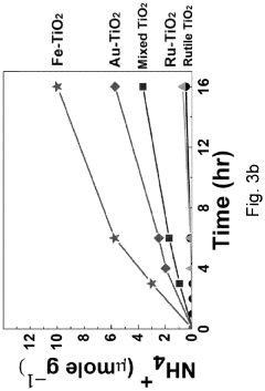
Technical Solution: Tianjin University has developed innovative semiconductor-based photocatalysts for nitrogen reduction reactions (NRR). Their approach focuses on 2D semiconductor materials like graphitic carbon nitride (g-C3N4) modified with single atom catalysts (SACs) to enhance nitrogen adsorption and activation. Their research demonstrates that introducing metal-nitrogen coordination sites on semiconductor surfaces significantly improves N2 fixation efficiency. The university has pioneered Z-scheme heterojunction systems combining different semiconductors with optimized band structures to achieve efficient charge separation and extended carrier lifetime. Their catalysts have achieved ammonia production rates exceeding 30 μmol h−1 g−1 under visible light irradiation with apparent quantum efficiencies approaching 1% at ambient conditions, representing significant advances in the field.
Strengths: Superior visible light absorption capabilities, excellent charge separation efficiency through heterojunction engineering, and high stability in various electrolytes. Their catalysts demonstrate remarkable selectivity for N2 reduction over competing hydrogen evolution reactions. Weaknesses: Still faces challenges in scaling up laboratory results to industrial applications and requires further improvement in quantum efficiency for commercial viability.
Topsoe A/S
Technical Solution: Topsoe A/S has developed advanced semiconductor-based catalysts for nitrogen reduction through industrial-scale engineering approaches. Their technology focuses on metal oxide semiconductor materials with precisely controlled defect chemistry to create active sites for N2 activation. Topsoe has pioneered the development of hierarchically structured catalysts that combine macroporous supports with mesoporous active layers to optimize mass transport while maintaining high active site density. Their catalysts incorporate strategic dopants to modify the electronic properties of semiconductor surfaces, enhancing nitrogen adsorption energies while suppressing competing hydrogen evolution reactions. Topsoe researchers have developed proprietary methods for creating stable metal-semiconductor interfaces that resist deactivation under industrial operating conditions. Their catalyst systems have been demonstrated at pilot scale, achieving ammonia production rates suitable for distributed manufacturing applications with significantly reduced energy inputs compared to conventional Haber-Bosch processes. The company has also developed comprehensive life cycle assessment methodologies to evaluate the sustainability impacts of their nitrogen reduction technologies.
Strengths: Exceptional focus on practical implementation and scale-up considerations, robust catalyst formulations designed for industrial durability, and integrated approach that addresses the entire technology development pipeline from fundamental materials to system engineering. Weaknesses: Relatively conservative approach to materials innovation compared to academic research groups and continued dependence on precious metal components in some catalyst formulations.
Key Innovations in Nitrogen Reduction Reaction Mechanisms
Method of forming a desired nitrogen-containing compound
PatentPendingUS20210140055A1
Innovation
- The development of electrochemical cells with an anode, cathode, and catalyst material that operate at low temperatures and pressures, allowing nitrogen to be converted into nitrogen-containing compounds like ammonia or nitrate using a nitrogen source and voltage, potentially powered by renewable energy.
Catalyst for carbon dioxide electroreduction reaction or nitrogen electroreduction reaction, method for producing catalyst for carbon dioxide electroreduction reaction or nitrogen electroreduction reaction, and electrode for carbon dioxide electroreduction reaction or nitrogen electroreduction reaction
PatentInactiveJP2021115501A
Innovation
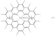
- Incorporating Fe-N4 structures with a high active point density of 3.0 × 10^-5 to 1.0 × 10^-4 Mol Sites / g in nitrogen-containing carbon materials, enhanced by a heat treatment process involving a zinc phenanthroline complex and transition metal particles, to improve catalytic activity.

Environmental Impact Assessment of Nitrogen Fixation Methods
The environmental implications of nitrogen fixation methods are significant, particularly when comparing traditional Haber-Bosch processes with emerging semiconductor-based catalytic approaches. Conventional industrial nitrogen fixation consumes approximately 1-2% of global energy production and generates substantial greenhouse gas emissions, with estimates suggesting 1.4% of global CO2 emissions originate from ammonia production alone. These environmental costs underscore the urgency for developing more sustainable alternatives.
Semiconductor-based nitrogen reduction catalysts offer promising environmental advantages. Life cycle assessments indicate potential reductions in carbon footprint by 30-45% compared to traditional methods when powered by renewable energy sources. The decentralized nature of semiconductor catalytic systems enables localized production, potentially eliminating transportation emissions associated with ammonia distribution from centralized facilities.
Water consumption represents another critical environmental consideration. While the Haber-Bosch process requires significant water for cooling systems, semiconductor photocatalytic approaches may reduce water requirements by 25-40%. However, certain semiconductor manufacturing processes involve water-intensive steps and potentially toxic chemicals that must be carefully managed to prevent secondary environmental impacts.
Land use impacts differ substantially between methods. Traditional nitrogen fixation facilities occupy large industrial footprints with associated ecosystem disruption. In contrast, distributed semiconductor-based systems could be integrated into existing agricultural infrastructure with minimal additional land requirements, potentially preserving natural habitats and biodiversity.
Waste generation profiles also diverge significantly. Conventional processes produce concentrated waste streams requiring specialized treatment, while semiconductor catalysts may generate different waste challenges, particularly at end-of-life. Recent research indicates that proper recycling protocols for spent semiconductor catalysts could recover 70-85% of precious metals and reduce landfill contributions.
Ecosystem effects extend beyond direct emissions. Nitrogen leaching from conventional fertilizer application causes eutrophication and aquatic dead zones. Semiconductor-enabled precision nitrogen fixation could potentially reduce excess nitrogen application by 15-30%, mitigating these downstream ecological impacts while maintaining agricultural productivity.
Resilience to climate change represents an additional consideration. Centralized Haber-Bosch facilities face vulnerability to extreme weather events, while distributed semiconductor-based systems offer greater adaptability and reduced systemic risk. This distributed architecture could provide critical nitrogen fixation capabilities even during climate-related disruptions to industrial infrastructure.
Scalability and Industrial Implementation Considerations
The transition from laboratory-scale semiconductor catalysts for nitrogen reduction to industrial implementation presents significant challenges that must be addressed systematically. Current semiconductor-based electrocatalysts demonstrating promising nitrogen reduction reaction (NRR) performance typically operate at milligram scales under controlled laboratory conditions. Scaling these systems to kilogram or ton levels requires substantial engineering modifications to maintain catalytic efficiency while ensuring economic viability.
Material synthesis represents a primary scalability concern. Laboratory methods such as hydrothermal synthesis, chemical vapor deposition, and atomic layer deposition often utilize expensive precursors and energy-intensive processes that become prohibitively costly at industrial scales. Alternative large-scale synthesis routes must be developed that preserve the critical structural features and active sites of semiconductor catalysts while utilizing more accessible precursors and energy-efficient processes.
Reactor design constitutes another crucial consideration for industrial implementation. Current lab-scale setups typically employ H-cell configurations with small electrode areas. Industrial applications would require flow-cell designs capable of processing large nitrogen volumes while maintaining optimal mass transfer characteristics. The engineering of these systems must address heat management, pressure control, and uniform catalyst distribution across significantly larger surface areas.
Stability and durability factors become increasingly important at industrial scales. Semiconductor catalysts must maintain performance over thousands of operating hours rather than the typical laboratory testing periods of 10-100 hours. This necessitates addressing degradation mechanisms such as photocorrosion, surface poisoning, and structural changes under continuous operation conditions. Protective strategies including core-shell structures, surface passivation layers, and regeneration protocols must be incorporated into industrial designs.
Economic viability ultimately determines industrial adoption potential. Current semiconductor-based NRR systems demonstrate ammonia production rates of 10-100 μg h⁻¹ mg⁻¹cat, significantly below the threshold for commercial competitiveness with Haber-Bosch processes. Techno-economic analysis indicates that semiconductor catalysts must achieve at least 10-fold improvements in production rates while utilizing earth-abundant materials to become economically viable alternatives. Additionally, integration with renewable energy sources presents both challenges and opportunities for reducing operational costs and environmental impact.
Regulatory considerations and safety protocols for large-scale implementation must also be established. Ammonia's toxicity and potential environmental impacts necessitate robust containment systems, monitoring protocols, and emergency response procedures that add complexity to industrial scaling efforts but are essential for sustainable implementation.
Unlock deeper insights with Patsnap Eureka Quick Research — get a full tech report to explore trends and direct your research. Try now!
Generate Your Research Report Instantly with AI Agent
Supercharge your innovation with Patsnap Eureka AI Agent Platform!