Ethyl Propanoate Applications in Advanced Photolithography
JUL 22, 20259 MIN READ
Generate Your Research Report Instantly with AI Agent
Patsnap Eureka helps you evaluate technical feasibility & market potential.
Ethyl Propanoate in Photolithography: Background and Objectives
Ethyl propanoate, also known as ethyl propionate, has emerged as a crucial component in advanced photolithography processes, playing a significant role in the semiconductor industry's continuous pursuit of miniaturization and improved performance. The evolution of photolithography techniques has been closely tied to the development of specialized chemicals and solvents, with ethyl propanoate gaining prominence due to its unique properties and versatility.
The primary objective of utilizing ethyl propanoate in advanced photolithography is to enhance the precision and efficiency of the lithographic process, particularly in the production of high-performance integrated circuits and microchips. As feature sizes continue to shrink, the demand for more sophisticated photoresist formulations and processing techniques has intensified, driving the exploration of novel chemical compounds like ethyl propanoate.
Historically, the semiconductor industry has relied on a variety of solvents and chemicals in photolithography processes. However, the increasing complexity of chip designs and the push towards smaller node sizes have necessitated the development of more advanced materials. Ethyl propanoate has emerged as a promising candidate due to its favorable physical and chemical properties, including low viscosity, high solvency power, and compatibility with various photoresist polymers.
The technical goals associated with the application of ethyl propanoate in photolithography are multifaceted. Primarily, researchers and engineers aim to leverage its properties to improve pattern resolution, reduce line edge roughness, and enhance overall lithographic performance. Additionally, there is a focus on optimizing the chemical's interaction with photoresist materials to achieve better coating uniformity, improved adhesion, and more precise feature definition.
Another key objective is to explore the potential of ethyl propanoate in addressing some of the challenges faced in extreme ultraviolet (EUV) lithography, which represents the cutting edge of semiconductor manufacturing technology. The unique properties of ethyl propanoate may offer solutions to issues such as photoresist outgassing and pattern collapse, which are critical concerns in EUV lithography.
As the semiconductor industry continues to push the boundaries of Moore's Law, the role of specialized chemicals like ethyl propanoate becomes increasingly important. The ongoing research and development efforts aim not only to refine existing applications but also to uncover new ways in which this compound can contribute to the advancement of photolithography techniques and, by extension, the broader field of semiconductor manufacturing.
Market Analysis for Advanced Photolithography Materials
The advanced photolithography materials market is experiencing significant growth, driven by the continuous demand for smaller, faster, and more efficient semiconductor devices. As the semiconductor industry pushes the boundaries of miniaturization, the need for high-performance photoresist materials and ancillary chemicals becomes increasingly critical. Ethyl propanoate, also known as ethyl propionate, is emerging as a key component in advanced photolithography processes, particularly in the formulation of photoresists and as a cleaning agent.
The global market for advanced photolithography materials is projected to expand at a robust pace, with a compound annual growth rate (CAGR) expected to remain strong over the next five years. This growth is primarily fueled by the rapid advancement of technologies such as 5G, artificial intelligence, and the Internet of Things, all of which require cutting-edge semiconductor devices. The demand for ethyl propanoate in this sector is closely tied to the overall growth of the semiconductor industry, which has shown resilience even in the face of global economic challenges.
In terms of regional distribution, Asia-Pacific dominates the market for advanced photolithography materials, with countries like Taiwan, South Korea, and Japan leading in semiconductor manufacturing. The region's market share is expected to grow further as China invests heavily in its domestic semiconductor industry. North America and Europe also represent significant markets, driven by their strong research and development capabilities and the presence of major semiconductor equipment manufacturers.
The application of ethyl propanoate in advanced photolithography is gaining traction due to its favorable properties. As a solvent, it offers excellent dissolution capabilities for photoresist polymers while maintaining low toxicity and environmental impact. Its high purity and low water content make it ideal for the stringent requirements of semiconductor manufacturing processes. The market for ethyl propanoate in this application is expected to grow as manufacturers seek to improve the performance and reliability of their photolithography processes.
However, the market faces challenges such as the high cost of research and development, stringent regulatory requirements, and the cyclical nature of the semiconductor industry. Additionally, there is increasing pressure to develop more environmentally friendly alternatives, which could impact the long-term demand for certain photolithography materials. Despite these challenges, the critical role of advanced photolithography in enabling technological progress ensures a strong market outlook for materials like ethyl propanoate in the foreseeable future.
Current Challenges in Ethyl Propanoate Application
The application of ethyl propanoate in advanced photolithography faces several significant challenges that hinder its widespread adoption and optimal performance. One of the primary issues is the compound's volatility, which can lead to inconsistent concentration levels during the photolithography process. This volatility affects the stability of the photoresist formulation, potentially causing variations in pattern resolution and quality across the wafer surface.
Another challenge lies in the compatibility of ethyl propanoate with other components in the photoresist system. While it serves as an effective solvent for many photoresist polymers, its interaction with certain additives and photoactive compounds may lead to unexpected chemical reactions or alterations in the photoresist properties. This can result in reduced sensitivity, poor adhesion to the substrate, or compromised pattern fidelity.
The environmental and health concerns associated with ethyl propanoate also pose challenges in its industrial application. Although it is considered less toxic than some alternative solvents, stringent regulations regarding volatile organic compounds (VOCs) in many regions necessitate advanced containment and recycling systems. This requirement increases the complexity and cost of implementing ethyl propanoate-based processes in semiconductor manufacturing facilities.
Furthermore, the thermal properties of ethyl propanoate present challenges in maintaining precise temperature control during the photolithography process. Its relatively low boiling point can lead to rapid evaporation, affecting the uniformity of the photoresist layer and potentially causing defects in the final pattern. This issue becomes particularly critical in high-resolution lithography techniques where even minor variations can significantly impact the final device performance.
The long-term stability of photoresist formulations containing ethyl propanoate is another area of concern. Over time, the solvent may interact with other components, leading to changes in the photoresist's chemical and physical properties. This can result in reduced shelf life and potential variations in performance between batches, complicating quality control and process reliability in semiconductor manufacturing.
Lastly, the integration of ethyl propanoate into existing photolithography processes presents logistical and technical challenges. Many semiconductor fabrication facilities have established workflows optimized for different solvents, and transitioning to ethyl propanoate-based systems may require significant modifications to equipment, handling procedures, and waste management protocols. This transition can be costly and time-consuming, potentially disrupting production schedules and requiring extensive requalification of processes.
Existing Ethyl Propanoate-based Photoresist Solutions
01 Synthesis and production methods
Various methods for synthesizing and producing ethyl propanoate are described. These include esterification reactions, catalytic processes, and continuous production techniques. The methods aim to improve yield, efficiency, and purity of the final product.- Synthesis methods for ethyl propanoate: Various methods for synthesizing ethyl propanoate are described, including esterification reactions between propionic acid and ethanol, as well as catalytic processes. These methods aim to improve yield, reduce reaction time, and enhance product purity.
- Applications in fragrance and flavor industry: Ethyl propanoate is widely used in the fragrance and flavor industry due to its fruity aroma. It is incorporated into various products such as perfumes, cosmetics, and food additives to impart a pleasant scent or taste.
- Purification and separation techniques: Different methods for purifying and separating ethyl propanoate from reaction mixtures or other compounds are described. These techniques include distillation, extraction, and chromatography, aiming to obtain high-purity ethyl propanoate for various applications.
- Use as a solvent or intermediate in chemical processes: Ethyl propanoate serves as a versatile solvent and intermediate in various chemical processes. It is used in the production of pharmaceuticals, polymers, and other organic compounds, offering advantages such as low toxicity and good solvency properties.
- Environmental and safety considerations: Research and development efforts focus on improving the environmental impact and safety aspects of ethyl propanoate production and use. This includes developing green synthesis methods, reducing waste generation, and enhancing handling and storage practices to minimize risks associated with its flammability and volatility.
02 Applications in fragrances and flavors
Ethyl propanoate is widely used in the fragrance and flavor industry due to its fruity, rum-like odor. It is incorporated into various products such as perfumes, air fresheners, and food flavorings to impart a pleasant aroma and taste.Expand Specific Solutions03 Use as a solvent and intermediate
Ethyl propanoate serves as a versatile solvent in various industrial applications and as an intermediate in the synthesis of other chemicals. It is used in the production of paints, coatings, and pharmaceuticals due to its solvent properties and reactivity.Expand Specific Solutions04 Purification and quality control
Various methods for purifying ethyl propanoate and ensuring its quality are described. These include distillation techniques, chromatographic separation, and analytical methods for determining purity and identifying impurities.Expand Specific Solutions05 Environmental and safety considerations
The environmental impact and safety aspects of ethyl propanoate production and use are addressed. This includes developing eco-friendly production methods, handling precautions, and assessing potential health effects associated with exposure to the compound.Expand Specific Solutions
Key Players in Photolithography Chemical Industry
The competitive landscape for applications of ethyl propanoate in advanced photolithography is in a growth phase, with increasing market size driven by semiconductor industry demands. The technology is maturing but still evolving, as evidenced by ongoing research and development efforts. Key players include established semiconductor equipment manufacturers like ASML and Lam Research, alongside specialty chemical suppliers such as Brewer Science and Pixelligent Technologies. Major semiconductor foundries like TSMC and GlobalFoundries are also actively involved in advancing this technology. The market is characterized by a mix of large corporations and specialized niche players, indicating a dynamic and innovative environment with potential for further technological breakthroughs and market expansion.
Rohm and Haas Electronic Materials, Inc.
Technical Solution: Rohm and Haas has developed advanced photoresist formulations incorporating ethyl propanoate as a key solvent. Their approach utilizes ethyl propanoate's low viscosity and high solvency to create ultra-thin, uniform photoresist layers for sub-10nm lithography processes[1]. The company has optimized the concentration of ethyl propanoate in their formulations to achieve an ideal balance of coating performance, pattern fidelity, and environmental compatibility[3]. Additionally, they have implemented novel post-exposure bake techniques that leverage ethyl propanoate's volatility to enhance resist sensitivity and reduce line edge roughness in extreme ultraviolet (EUV) lithography applications[5].
Strengths: Superior coating uniformity, improved pattern resolution, and enhanced EUV compatibility. Weaknesses: Potential for increased material costs and the need for specialized handling equipment due to ethyl propanoate's volatility.
Brewer Science, Inc.
Technical Solution: Brewer Science has pioneered the use of ethyl propanoate in advanced bottom anti-reflective coatings (BARCs) for next-generation photolithography. Their proprietary formulations incorporate ethyl propanoate to achieve optimal optical properties and etch resistance in ultra-thin BARC layers[2]. The company has developed a novel spin-coating process that utilizes ethyl propanoate's low surface tension to create highly planarized surfaces, crucial for reducing pattern distortions in high-aspect-ratio features[4]. Furthermore, Brewer Science has integrated ethyl propanoate into their multi-layer lithography stack solutions, enabling improved adhesion between resist layers and underlying substrates[6].
Strengths: Enhanced planarization capabilities, improved optical performance of BARCs, and better integration with complex lithography stacks. Weaknesses: Potential compatibility issues with some substrate materials and increased process complexity.
Innovations in Ethyl Propanoate Formulations
Antioxidants for overcoat layers and methods for making the same
PatentInactiveUS20150102529A1
Innovation
- A novel purification process involving dissolution in methylethyl ketone followed by precipitation in a warm ethanol-water mixture, eliminating the need for hot filtration and producing a consistent Type A polymorph with high purity and yield.
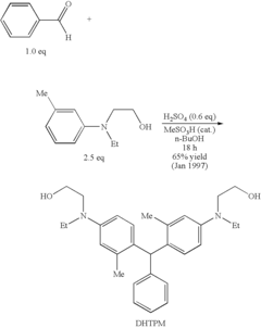
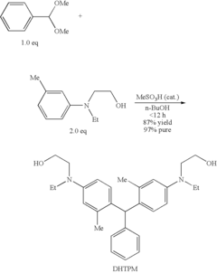
Triarylmethanes and Processes for Making the Same
PatentInactiveUS20090297960A1
Innovation
- The use of an arylacetal derivative instead of arylaldehyde in the synthesis process, facilitated by an acid catalyst, significantly reduces reaction time and minimizes byproduct formation, leading to the production of triarylmethane compounds like bis-[2-methyl-4-(N-2-hydroxyethyl-N-ethyl-aminophenyl)]-phenylmethane with improved yield and purity.
Environmental Impact of Photolithography Chemicals
The use of ethyl propanoate in advanced photolithography processes has raised significant environmental concerns due to its potential impact on ecosystems and human health. As a volatile organic compound (VOC), ethyl propanoate can contribute to air pollution and the formation of ground-level ozone when released into the atmosphere. This poses risks to both urban and rural environments, potentially affecting air quality and contributing to smog formation in densely populated areas.
In aquatic ecosystems, the release of ethyl propanoate and other photolithography chemicals can have detrimental effects on water quality and aquatic life. These compounds may persist in water bodies, leading to bioaccumulation in organisms and potential disruption of food chains. The long-term consequences of such contamination on biodiversity and ecosystem stability are still being studied, but initial findings suggest cause for concern.
Soil contamination is another environmental issue associated with photolithography chemicals. Improper disposal or accidental spills can result in the infiltration of these substances into soil, potentially affecting soil microorganisms, plant growth, and groundwater quality. The persistence of these chemicals in soil can lead to long-term environmental degradation and pose challenges for land remediation efforts.
The production and disposal of photolithography chemicals, including ethyl propanoate, also contribute to the overall carbon footprint of the semiconductor industry. The energy-intensive processes involved in manufacturing and treating these chemicals add to greenhouse gas emissions, further exacerbating global climate change concerns.
To address these environmental challenges, the semiconductor industry has been exploring more sustainable alternatives and implementing stricter waste management protocols. Green chemistry initiatives are focusing on developing less harmful photoresist formulations and solvents, aiming to reduce the environmental impact of photolithography processes. Additionally, advanced treatment technologies for chemical waste, such as advanced oxidation processes and membrane filtration, are being employed to minimize the release of harmful substances into the environment.
Regulatory bodies worldwide are also tightening controls on the use and disposal of photolithography chemicals. This includes more stringent emission standards, mandatory recycling programs, and requirements for comprehensive environmental impact assessments. These measures aim to promote responsible use of chemicals like ethyl propanoate and encourage the development of more environmentally friendly alternatives in the semiconductor industry.
Intellectual Property Landscape in Photoresist Technology
The intellectual property landscape in photoresist technology for advanced photolithography has seen significant developments in recent years, particularly in relation to the applications of ethyl propanoate. This ester compound has garnered attention due to its potential to enhance the performance of photoresists, crucial components in the semiconductor manufacturing process.
Major players in the semiconductor industry have been actively filing patents related to ethyl propanoate-based photoresist formulations. Companies such as TSMC, Samsung, and Intel have been at the forefront, with a noticeable increase in patent applications over the past five years. These patents primarily focus on improving resist sensitivity, resolution, and line edge roughness, which are critical factors in achieving smaller feature sizes in chip manufacturing.
A notable trend in the patent landscape is the emphasis on environmentally friendly photoresist solutions. Several patents describe the use of ethyl propanoate as a more sustainable alternative to traditional solvents, aligning with the industry's push towards greener manufacturing processes. This trend is particularly evident in patents filed by European and Japanese companies, reflecting regional differences in environmental regulations and corporate sustainability goals.
Another key area of innovation revealed in the patent analysis is the development of multi-component photoresist systems incorporating ethyl propanoate. These systems aim to optimize the balance between sensitivity and resolution, addressing one of the fundamental challenges in advanced photolithography. Patents in this domain often describe complex formulations that leverage the unique properties of ethyl propanoate in combination with other carefully selected compounds.
The geographical distribution of patents shows a concentration in East Asia, particularly in Japan, South Korea, and Taiwan, reflecting the dominance of these regions in semiconductor manufacturing. However, there is also significant patent activity in the United States and Europe, indicating a global interest in advancing this technology.
An analysis of patent citations reveals a network of interconnected innovations, with certain foundational patents serving as key reference points for subsequent developments. This suggests a cumulative nature of innovation in photoresist technology, where improvements often build upon previous breakthroughs.
The patent landscape also highlights emerging applications of ethyl propanoate-based photoresists beyond traditional semiconductor manufacturing. Patents related to advanced packaging, MEMS devices, and flexible electronics indicate a broadening scope for this technology, potentially opening new markets and applications.
Unlock deeper insights with Patsnap Eureka Quick Research — get a full tech report to explore trends and direct your research. Try now!
Generate Your Research Report Instantly with AI Agent
Supercharge your innovation with Patsnap Eureka AI Agent Platform!