Best Practices for Integration of Microfluidics and MEMS Sensors
SEP 10, 202510 MIN READ
Generate Your Research Report Instantly with AI Agent
Patsnap Eureka helps you evaluate technical feasibility & market potential.
Microfluidics-MEMS Integration Background and Objectives
Microfluidics and Micro-Electro-Mechanical Systems (MEMS) have evolved as separate technological domains over the past three decades, each with its own development trajectory and application focus. Microfluidics emerged in the early 1990s as a technology for manipulating small volumes of fluids through microscale channels, while MEMS technology dates back to the 1970s with the development of miniaturized mechanical components integrated with electronics on silicon substrates.
The convergence of these two technologies represents a natural evolution in miniaturization and system integration, driven by increasing demands for compact, multifunctional analytical and sensing platforms. This integration enables the development of complete lab-on-a-chip systems that can perform complex analytical tasks with minimal sample volumes, reduced reagent consumption, and accelerated analysis times.
Historical milestones in this integration journey include the first microfluidic valves in the late 1990s, the development of integrated pressure sensors for flow control in the early 2000s, and more recently, the emergence of comprehensive sensing platforms that combine multiple MEMS sensors with sophisticated microfluidic handling capabilities. Each advancement has progressively addressed challenges in interface compatibility, materials selection, and fabrication processes.
The current technological landscape shows a clear trend toward higher levels of integration, with particular emphasis on biomedical applications, environmental monitoring, and point-of-care diagnostics. These applications benefit significantly from the combination of precise fluid handling capabilities with sensitive detection mechanisms, enabling rapid, on-site analysis that was previously confined to laboratory settings.
The primary objective of microfluidics-MEMS integration is to establish standardized approaches that overcome persistent technical challenges, including material compatibility issues, packaging complexities, and interface optimization between fluidic and electronic components. Additionally, there is a growing focus on developing scalable manufacturing processes that can transition these integrated systems from research prototypes to commercial products.
Looking forward, the technology evolution trajectory points toward increasingly sophisticated integration strategies that will enable fully autonomous microsystems capable of sample preparation, analysis, and data processing within a single platform. This evolution is expected to be driven by advances in materials science, fabrication techniques, and system-level design methodologies that address the unique requirements of hybrid microfluidic-MEMS devices.
The ultimate goal is to establish best practices that facilitate the development of reliable, cost-effective integrated systems that can be deployed across diverse application domains, from healthcare and environmental monitoring to industrial process control and beyond.
Market Applications and Demand Analysis
The integration of microfluidics and MEMS sensors represents a rapidly growing market with diverse applications across multiple industries. The global microfluidics market was valued at $13.5 billion in 2019 and is projected to reach $44.0 billion by 2027, with a CAGR of 16.2%. When combined with MEMS sensor technology, this integrated approach addresses critical needs in healthcare, environmental monitoring, and industrial processes.
In the healthcare sector, demand for integrated microfluidic-MEMS solutions is primarily driven by point-of-care diagnostics, which enable rapid testing with minimal sample volumes. The COVID-19 pandemic has significantly accelerated this trend, with healthcare providers seeking portable, accurate diagnostic tools that can deliver results within minutes rather than hours or days. Lab-on-a-chip devices incorporating both microfluidics and sensing capabilities have seen particular growth in applications for blood analysis, pathogen detection, and drug delivery systems.
Pharmaceutical companies represent another major market segment, with increasing investment in microfluidic-MEMS platforms for drug discovery and development. These integrated systems enable high-throughput screening with significantly reduced reagent consumption, addressing both cost and efficiency concerns in the R&D process. Market analysis indicates that pharmaceutical applications will grow at a CAGR of 18.7% through 2025.
Environmental monitoring applications are expanding rapidly as regulatory requirements become more stringent worldwide. Water quality testing, air pollution monitoring, and soil analysis all benefit from integrated microfluidic-MEMS solutions that offer portability, sensitivity, and real-time data capabilities. This market segment is expected to grow at 15.3% annually, driven by both governmental regulations and increasing public awareness of environmental issues.
Industrial process control represents an emerging application area with substantial growth potential. The chemical, food and beverage, and oil and gas industries are increasingly adopting microfluidic-MEMS systems for real-time monitoring of production processes, quality control, and safety applications. These industries value the ability to perform continuous monitoring with minimal sample volumes and reduced waste generation.
Market analysis reveals regional variations in adoption patterns. North America currently leads the market with approximately 38% share, followed by Europe at 29% and Asia-Pacific at 24%. However, the Asia-Pacific region is expected to show the highest growth rate over the next five years due to increasing healthcare expenditure, expanding industrial base, and government initiatives supporting advanced manufacturing technologies.
Consumer demand is increasingly focused on systems that offer seamless integration, reduced form factors, and wireless connectivity. End-users across all sectors prioritize solutions that can be easily incorporated into existing workflows while providing improved performance metrics such as sensitivity, specificity, and response time.
Technical Challenges in Microfluidics-MEMS Integration
The integration of microfluidics and MEMS sensors presents significant technical challenges that must be addressed to achieve optimal system performance. One of the primary obstacles is material compatibility between the microfluidic components and MEMS sensors. Different materials exhibit varying chemical resistance, thermal expansion coefficients, and mechanical properties, which can lead to interface failures, leakage, or contamination issues. For instance, polymers commonly used in microfluidics may not be compatible with silicon-based MEMS fabrication processes.
Fabrication process integration poses another substantial challenge. Microfluidic systems typically employ soft lithography, hot embossing, or injection molding, while MEMS sensors rely on semiconductor fabrication techniques. These disparate manufacturing approaches create difficulties in establishing seamless integration protocols that maintain the integrity of both components. The temperature sensitivity of materials during fabrication can cause warping, delamination, or stress-induced failures at integration points.
Scale mismatch between microfluidic channels and MEMS sensing elements presents additional complications. Microfluidic channels typically operate at dimensions of tens to hundreds of micrometers, while many MEMS sensors function optimally at smaller scales. This dimensional incongruity necessitates careful interface design to ensure efficient fluid delivery to sensing regions without compromising detection sensitivity or increasing dead volumes.
Signal transduction and noise management represent critical challenges in integrated systems. Fluid-based interference can introduce noise into electrical measurements, while electrical components may affect fluid behavior through phenomena such as electrolysis or joule heating. Developing effective isolation strategies and signal processing algorithms is essential for maintaining measurement accuracy in these hybrid systems.
Packaging and encapsulation difficulties further complicate integration efforts. Integrated systems must simultaneously protect electronic components from fluid exposure while allowing controlled fluid access to sensing elements. This paradoxical requirement demands sophisticated packaging solutions that can withstand the mechanical stresses of fluid flow while maintaining electrical connections and preventing contamination.
Reliability and lifetime considerations present ongoing challenges. Integrated microfluidic-MEMS systems often experience degradation mechanisms not present in either technology independently. These include biofouling at sensor interfaces, material fatigue from repeated fluid cycling, and chemical compatibility issues over extended operation periods. Developing accelerated testing protocols that accurately predict long-term performance remains an unresolved challenge.
Standardization gaps across the microfluidics and MEMS industries further impede integration efforts. Unlike the semiconductor industry, microfluidics lacks universally accepted design rules, interface specifications, and testing protocols. This absence of standards complicates component interoperability and hinders the development of modular approaches to system integration.
Current Integration Methodologies and Solutions
01 Microfluidic device fabrication and integration with MEMS sensors
Techniques for fabricating microfluidic devices integrated with MEMS sensors involve specialized manufacturing processes that ensure compatibility between the fluid handling components and sensing elements. These methods include microfabrication techniques such as photolithography, etching, and bonding to create channels, chambers, and sensor structures on a single substrate. The integration allows for precise fluid control while maintaining high sensitivity detection capabilities, enabling applications in chemical analysis and biomedical diagnostics.- Microfluidic device fabrication and integration with MEMS sensors: Techniques for fabricating microfluidic devices that integrate with MEMS sensors, including methods for creating channels, chambers, and sensor interfaces. These approaches focus on material selection, bonding techniques, and microfabrication processes that enable seamless integration of sensing elements within microfluidic platforms. The integration allows for precise fluid handling while maintaining sensor functionality and sensitivity.
- Flow control and fluid manipulation in integrated systems: Methods for controlling fluid flow in microfluidic-MEMS integrated systems, including valve designs, pumping mechanisms, and flow regulation techniques. These approaches enable precise manipulation of small fluid volumes while maintaining compatibility with integrated sensing elements. Advanced flow control mechanisms allow for automated sample processing, reagent mixing, and controlled reaction environments within the integrated platforms.
- Signal processing and data acquisition from integrated sensors: Techniques for processing signals and acquiring data from MEMS sensors integrated within microfluidic platforms. These approaches address challenges related to noise reduction, signal amplification, and data interpretation from sensors operating in fluid environments. Advanced signal processing methods enable real-time monitoring and feedback control in integrated microfluidic-MEMS systems.
- Packaging and encapsulation techniques for microfluidic-MEMS systems: Methods for packaging and encapsulating integrated microfluidic-MEMS systems to ensure reliability, biocompatibility, and protection from environmental factors. These techniques address challenges related to hermetic sealing, electrical connections, and fluidic interfaces while maintaining sensor functionality. Advanced packaging approaches enable practical deployment of integrated systems in various application environments.
- Lab-on-chip platforms with integrated sensing capabilities: Development of complete lab-on-chip platforms that integrate multiple microfluidic functions with various MEMS sensing modalities. These integrated systems combine sample preparation, fluid handling, reaction chambers, and detection capabilities on a single platform. The integration enables complex analytical procedures to be performed with minimal sample volumes and reduced analysis time, suitable for point-of-care diagnostics and environmental monitoring applications.
02 Sensor arrays and multiplexed detection systems
Microfluidic platforms incorporating arrays of MEMS sensors enable multiplexed detection capabilities for simultaneous analysis of multiple parameters or samples. These systems utilize sensor arrays strategically positioned within microfluidic channels to monitor various physical, chemical, or biological parameters in real-time. The integration of multiple sensing elements enhances analytical throughput and provides comprehensive data collection, making these systems valuable for applications requiring multi-parameter analysis such as environmental monitoring and medical diagnostics.Expand Specific Solutions03 Flow control and fluid manipulation in integrated systems
Advanced flow control mechanisms are essential in integrated microfluidic-MEMS systems to precisely manipulate small fluid volumes. These mechanisms include micropumps, microvalves, and flow regulators that can be controlled electronically to direct fluid movement through complex channel networks. The integration of these flow control elements with sensing components enables dynamic sample processing, reagent mixing, and automated analytical procedures, improving the functionality and versatility of lab-on-a-chip devices.Expand Specific Solutions04 Packaging and interconnection technologies
Specialized packaging and interconnection technologies are crucial for creating robust microfluidic-MEMS integrated systems. These technologies address challenges related to electrical connections, fluidic interfaces, and environmental protection while maintaining the microscale dimensions of the devices. Advanced packaging approaches include wafer-level bonding, 3D integration, and modular designs that facilitate both electrical and fluidic connections. Proper packaging ensures reliable operation, prevents contamination, and extends device lifetime in various application environments.Expand Specific Solutions05 Material selection and compatibility considerations
Material selection is critical for successful integration of microfluidics with MEMS sensors, requiring consideration of chemical compatibility, mechanical properties, and fabrication constraints. Materials must withstand exposure to various fluids while maintaining sensor functionality and preventing contamination or degradation. Common materials include silicon, glass, polymers like PDMS, and specialized coatings that provide biocompatibility or chemical resistance. Strategic material choices enable optimal performance in specific applications such as biological analysis, chemical sensing, or environmental monitoring.Expand Specific Solutions
Leading Companies and Research Institutions
The integration of microfluidics and MEMS sensors is currently in a growth phase, with the market expected to reach significant expansion due to increasing applications in healthcare, environmental monitoring, and industrial automation. Major players like Honeywell International, Abbott Laboratories, and IBM are driving innovation through substantial R&D investments, while specialized entities such as Coventor and X-FAB are advancing fabrication techniques. Academic institutions including Technion Research Foundation and Southeast University contribute fundamental research. The technology is approaching maturity in certain applications, with companies like STMicroelectronics and Goertek Microelectronics leading commercial implementation. However, challenges in standardization and manufacturing scalability remain, creating opportunities for emerging players to establish competitive advantages through novel integration approaches.
Honeywell International Technologies Ltd.
Technical Solution: Honeywell has developed an integrated microfluidic-MEMS platform that combines pressure, temperature, and flow sensing capabilities within a single chip architecture. Their approach utilizes silicon micromachining techniques to create multi-layer fluidic channels directly interfaced with MEMS sensor elements. The platform employs a unique packaging solution that hermetically seals the electronic components while providing robust fluidic interconnects. Honeywell's integration methodology focuses on minimizing thermal gradients across the sensing elements by implementing proprietary compensation algorithms and structural design elements. Their systems typically incorporate redundant sensing elements and self-diagnostic capabilities to ensure reliability in critical applications such as aerospace and industrial process control. The company has demonstrated successful implementation in high-pressure differential applications with accuracy levels of ±0.1% of full scale.
Strengths: Exceptional reliability in harsh environments with proven long-term stability; advanced compensation techniques for temperature and pressure variations; comprehensive self-diagnostic capabilities. Weaknesses: Higher cost structure compared to consumer-grade solutions; relatively larger form factor than some competing technologies; proprietary interfaces may limit interoperability with third-party systems.
Coventor, Inc.
Technical Solution: Coventor has pioneered a comprehensive design-to-manufacturing approach for microfluidic-MEMS integration through their CoventorMP and MEMS+ platforms. Their technology enables multi-physics simulation of coupled fluidic-mechanical-electrical domains, allowing engineers to predict system behavior before physical prototyping. Coventor's methodology addresses the critical challenge of interface design between microfluidic channels and sensing elements by utilizing specialized transition regions that minimize stress concentration and potential failure points. Their platform supports various fabrication techniques including deep reactive ion etching (DRIE), surface micromachining, and soft lithography, providing flexibility in material selection and process optimization. The company has developed specific design rules and verification tools that account for the unique challenges of microfluidic-MEMS integration, such as surface tension effects, capillary forces, and fluid-structure interactions. Their simulation capabilities extend to predicting long-term reliability issues such as material fatigue and chemical compatibility.
Strengths: Industry-leading simulation capabilities for multi-physics modeling; comprehensive design rule checking specific to microfluidic-MEMS integration; supports multiple fabrication methodologies. Weaknesses: Steep learning curve for effective utilization of the software suite; computationally intensive simulations may require significant hardware resources; primarily focused on design rather than providing complete manufacturing solutions.
Key Patents and Technical Innovations
Microfluidic system and method for manufacturing the same
PatentInactiveEP2307137A2
Innovation
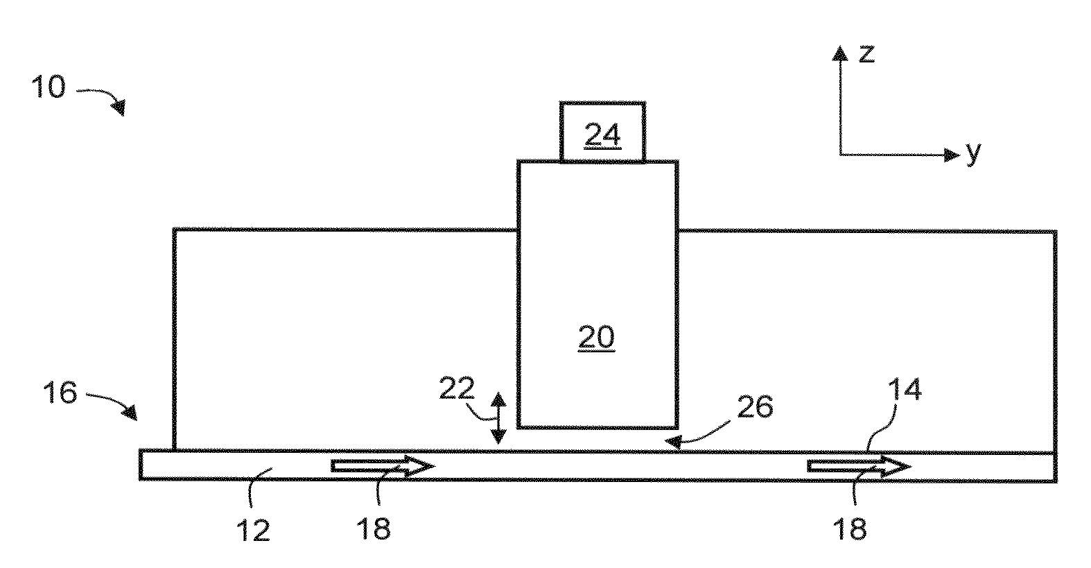
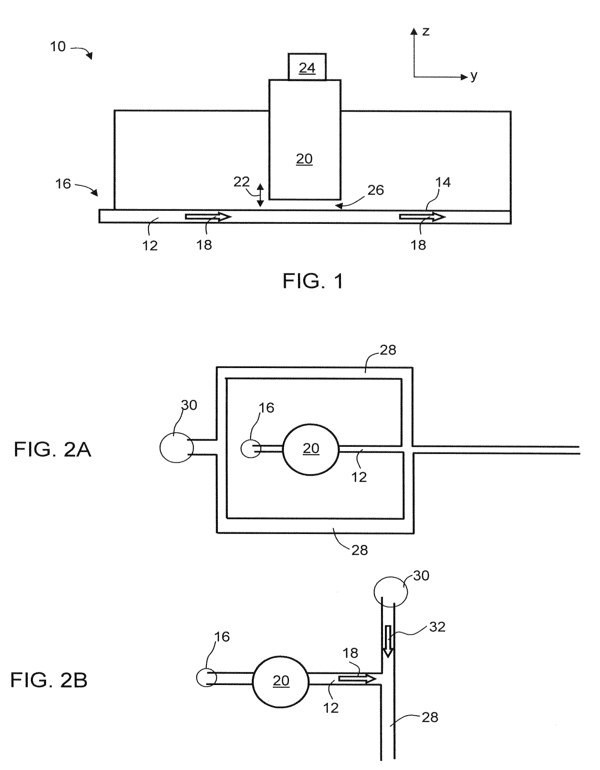
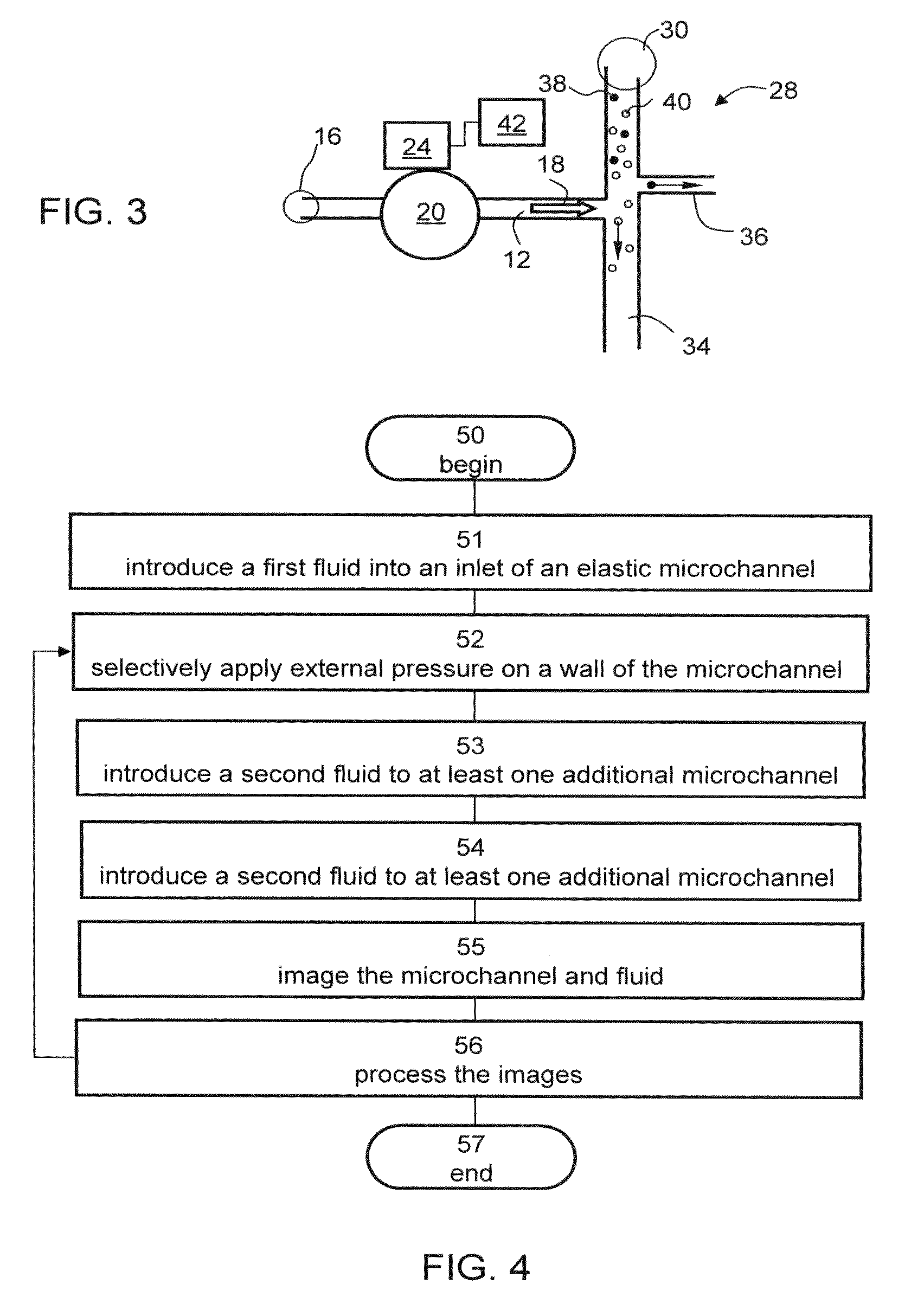
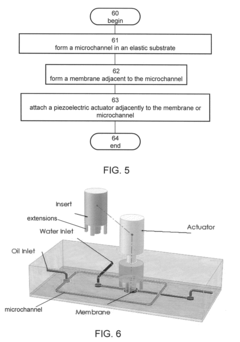
- A microfluidic system with an elastic microchannel and a piezoelectric actuator that applies external pressure to control fluid flow, allowing for precise manipulation of droplet generation by varying the actuator's displacement and voltage, enabling uniform droplet size and shape with a standard deviation of less than 1%.
Microfluidic system and method for manufacturing the same
PatentInactiveUS20100018584A1
Innovation
- A microfluidic system with an elastic microchannel and a piezoelectric actuator that applies external pressure to control fluid flow, allowing for the generation of droplets of uniform size and shape by varying the actuator's displacement and voltage, enabling independent control of droplet parameters.
Materials Compatibility and Fabrication Processes
The integration of microfluidics and MEMS sensors presents significant challenges in materials compatibility and fabrication processes. Silicon, glass, and polymers constitute the primary materials used in these integrated systems, each offering distinct advantages and limitations. Silicon provides excellent mechanical properties and established fabrication techniques compatible with MEMS processing, but presents challenges in bonding with polymer microfluidic components. Glass offers superior optical transparency and chemical resistance, making it ideal for applications requiring visual inspection or fluorescence detection, though its processing costs exceed those of polymers.
Polymers such as PDMS (polydimethylsiloxane), PMMA (polymethyl methacrylate), and COC (cyclic olefin copolymer) have gained prominence due to their cost-effectiveness and fabrication flexibility. PDMS particularly stands out for rapid prototyping through soft lithography, though it suffers from solvent absorption and potential leaching of uncured oligomers that may interfere with sensor performance. COC offers superior chemical resistance and optical properties, making it increasingly popular for commercial applications.
Surface modification techniques play a crucial role in ensuring compatibility between different materials. Plasma treatment, silanization, and UV-ozone exposure can modify surface properties to enhance bonding between dissimilar materials and control surface wettability—critical for predictable fluid behavior in microchannels. These treatments must be carefully optimized to avoid compromising sensor functionality or introducing contamination.
Fabrication processes must be carefully sequenced to preserve the integrity of both microfluidic channels and electronic components. The "MEMS-first" approach involves completing all high-temperature MEMS processing before introducing temperature-sensitive microfluidic components, while "microfluidics-first" strategies may be preferred when channel geometry precision is paramount. Hybrid approaches utilizing sacrificial layers to protect sensitive components during processing have shown promising results in recent research.
Bonding technologies represent another critical consideration, with anodic bonding preferred for silicon-glass interfaces, while adhesive bonding or thermal fusion bonding often serves polymer-based systems. Emerging techniques such as localized laser bonding offer advantages for temperature-sensitive components by minimizing heat exposure to critical sensor areas.
Standardization efforts are gradually emerging to address reproducibility challenges, with organizations like NIST developing reference materials and measurement protocols. However, the field still lacks comprehensive standards for materials testing and process validation, presenting opportunities for industry leadership in establishing best practices for integrated microfluidic-MEMS fabrication.
Standardization and Quality Control Frameworks
The integration of microfluidics and MEMS sensors requires robust standardization and quality control frameworks to ensure reliability, reproducibility, and interoperability across different manufacturing processes and applications. Currently, the field suffers from fragmentation in standards, with various organizations proposing different guidelines that often lack harmonization. The IEEE, ASTM International, and ISO have developed preliminary standards addressing aspects of MEMS fabrication and microfluidic device characterization, but comprehensive frameworks specifically for integrated systems remain underdeveloped.
Effective standardization frameworks must address multiple dimensions: dimensional specifications, material properties, interface protocols, and performance metrics. For microfluidic-MEMS integration, critical parameters include channel dimensions, flow rates, pressure tolerances, sensor response times, and cross-contamination limits. The establishment of reference materials and calibration protocols is essential for ensuring measurement traceability and comparability between different laboratories and manufacturing facilities.
Quality control methodologies for integrated microfluidic-MEMS systems typically involve multi-stage testing protocols. Initial screening focuses on individual component functionality, followed by integration testing that evaluates system-level performance. Non-destructive testing techniques such as optical coherence tomography, electrical impedance spectroscopy, and fluorescence-based flow visualization have emerged as valuable tools for in-process quality assessment without compromising device integrity.
Statistical process control (SPC) approaches adapted specifically for microfluidic-MEMS manufacturing environments show promising results in reducing batch-to-batch variability. Implementation of Six Sigma methodologies has demonstrated up to 30% improvement in yield rates for complex integrated devices, particularly when combined with automated inspection systems utilizing machine vision algorithms trained on defect libraries.
Documentation standards represent another critical aspect of quality frameworks. The development of standardized device passports that capture manufacturing parameters, quality control results, and performance characteristics enables better traceability throughout the product lifecycle. These documentation protocols facilitate regulatory compliance, particularly important for medical and pharmaceutical applications where microfluidic-MEMS devices face stringent approval requirements.
Collaborative industry-academic initiatives are working to establish open-source reference designs and testing protocols that could accelerate standardization efforts. The Microfluidic Open Technology Consortium and the MEMS Industry Group have jointly proposed a roadmap for standardization that emphasizes interoperability between components from different manufacturers, potentially transforming the current fragmented ecosystem into a more modular, plug-and-play environment similar to what exists in conventional electronics.
Unlock deeper insights with Patsnap Eureka Quick Research — get a full tech report to explore trends and direct your research. Try now!
Generate Your Research Report Instantly with AI Agent
Supercharge your innovation with Patsnap Eureka AI Agent Platform!