

Enhancing Microfluidic Design for Large-Scale Manufacturability
SEP 10, 202510 MIN READ
Generate Your Research Report Instantly with AI Agent
Patsnap Eureka helps you evaluate technical feasibility & market potential.
Microfluidic Technology Evolution and Objectives
Microfluidic technology has evolved significantly since its inception in the early 1990s, transforming from simple channel designs to sophisticated lab-on-a-chip systems. The initial development phase focused primarily on proof-of-concept demonstrations in academic settings, utilizing materials like polydimethylsiloxane (PDMS) for rapid prototyping. These early systems established fundamental principles but lacked standardization and scalability necessary for industrial applications.
By the early 2000s, the field witnessed a paradigm shift toward practical applications, particularly in biomedical diagnostics and pharmaceutical research. This period marked the emergence of integrated microfluidic platforms incorporating multiple functionalities such as mixing, separation, and detection within a single device. Despite these advances, manufacturing remained largely artisanal, with limited throughput and reproducibility.
The current technological landscape is characterized by increasing convergence with adjacent fields including materials science, nanotechnology, and artificial intelligence. Modern microfluidic systems employ sophisticated design principles such as droplet microfluidics, inertial microfluidics, and digital microfluidics, enabling unprecedented control over fluid behavior at the microscale. However, a significant gap persists between laboratory demonstrations and industrial-scale production capabilities.
The primary objective of enhancing microfluidic design for large-scale manufacturability is to bridge this translational gap by developing robust, cost-effective fabrication methodologies that maintain precision while enabling high-volume production. This necessitates addressing several interconnected challenges: material selection that balances performance with processability, design optimization for manufacturing constraints, and development of standardized interfaces for system integration.
A parallel objective involves establishing design frameworks that incorporate manufacturing considerations from the outset, rather than as an afterthought. This "design for manufacturability" approach requires comprehensive understanding of how geometric features, material properties, and process parameters interact to determine device performance and production yield.
Looking forward, the field aims to achieve several ambitious milestones: reducing unit production costs by an order of magnitude while maintaining or improving performance specifications; developing automated quality control methodologies specific to microfluidic manufacturing; and establishing industry-wide standards for design, materials, and testing protocols. These objectives collectively support the ultimate goal of transitioning microfluidic technology from specialized applications to mainstream adoption across multiple industries.
The evolution trajectory suggests that successful large-scale manufacturability will likely emerge from convergent innovations in materials processing, automation technologies, and computational design tools, rather than from incremental improvements in any single domain.
Market Analysis for Scalable Microfluidic Solutions
The global microfluidics market is experiencing robust growth, projected to reach $42.7 billion by 2027, with a compound annual growth rate (CAGR) of 16.2% from 2022. This significant expansion is driven primarily by increasing applications in pharmaceutical research, point-of-care diagnostics, and life science research. The COVID-19 pandemic has further accelerated market growth by highlighting the critical importance of rapid, portable diagnostic solutions that microfluidic technologies can deliver.
Healthcare applications currently dominate the market landscape, accounting for approximately 60% of total market share. Within this segment, point-of-care testing represents the fastest-growing application area with a CAGR of 18.7%, as healthcare systems worldwide seek more efficient and decentralized testing capabilities. The pharmaceutical industry follows closely, with growing adoption of microfluidic technologies for drug discovery and development processes, reducing both time and costs associated with traditional methods.
Geographically, North America leads the market with 38% share, followed by Europe (29%) and Asia-Pacific (24%). However, the Asia-Pacific region is expected to witness the highest growth rate over the next five years due to increasing healthcare infrastructure investments, particularly in China and India, and the establishment of manufacturing hubs that can support large-scale microfluidic device production.
Customer demand is increasingly focused on scalable manufacturing solutions that can bridge the gap between laboratory prototypes and mass-produced commercial products. End-users across industries report that current manufacturing limitations represent the primary barrier to wider adoption, with 72% of potential industrial users citing manufacturing scalability as their top concern when considering microfluidic technology implementation.
The market shows clear segmentation between high-value, low-volume applications (such as specialized research tools) and low-cost, high-volume products (like disposable diagnostic devices). The latter category presents the greatest opportunity for growth but faces the most significant manufacturing challenges. Industry surveys indicate that reducing unit costs by 40-60% through improved manufacturing processes would trigger widespread adoption across multiple sectors.
Key customer requirements emerging from market research include: standardization of components and interfaces to enable modular design approaches; materials that maintain performance while supporting high-throughput manufacturing methods; and automated quality control systems capable of ensuring consistency across large production volumes. Additionally, sustainability concerns are becoming increasingly important, with 65% of potential customers expressing preference for environmentally friendly materials and manufacturing processes.
Current Limitations in Large-Scale Microfluidic Manufacturing
Despite significant advancements in microfluidic technology over the past two decades, large-scale manufacturing remains a critical bottleneck that impedes widespread commercial adoption. Traditional fabrication methods such as soft lithography using polydimethylsiloxane (PDMS) are well-suited for prototyping and small-batch production but present substantial challenges when scaled to industrial volumes. These methods typically require clean room facilities, specialized equipment, and highly trained personnel, resulting in high production costs and limited throughput.
Material limitations constitute another significant barrier to large-scale manufacturing. PDMS, while advantageous for prototyping due to its optical transparency and gas permeability, exhibits properties that complicate mass production, including absorption of small hydrophobic molecules, susceptibility to swelling when exposed to organic solvents, and challenges in achieving consistent surface properties across large production batches. Alternative materials like thermoplastics offer better manufacturability but often compromise on the performance characteristics that make PDMS attractive for research applications.
Standardization issues further complicate large-scale production efforts. The microfluidic industry lacks unified design standards and protocols, resulting in fragmented approaches to device design and manufacturing. This absence of standardization creates difficulties in transferring designs from research laboratories to manufacturing facilities and hampers the development of automated production processes that could significantly reduce costs and increase throughput.
Integration challenges between microfluidic components and external systems represent another substantial limitation. Current manufacturing processes struggle to efficiently incorporate elements such as sensors, actuators, and electronic components into microfluidic devices at scale. This integration complexity increases production costs and failure rates while limiting the functionality of mass-produced devices compared to their laboratory counterparts.
Quality control presents unique challenges in microfluidic manufacturing due to the microscale dimensions of critical features. Conventional inspection methods often lack the resolution or throughput necessary for efficient production line implementation. Defects that might be acceptable in prototype devices can significantly impact performance in commercial applications, necessitating more sophisticated and automated quality assurance processes that are currently underdeveloped.
Supply chain constraints further complicate scaling efforts. The specialized nature of microfluidic components and materials has resulted in a limited supplier ecosystem, creating vulnerabilities in production pipelines and contributing to higher costs. Many manufacturers rely on custom-built equipment and proprietary processes, which inhibits knowledge sharing and standardization across the industry.
Addressing these limitations requires coordinated efforts across multiple domains, including materials science, manufacturing engineering, and industry standardization initiatives. Recent developments in 3D printing, injection molding adaptations, and roll-to-roll processing show promise for overcoming some of these challenges, but significant work remains to establish truly scalable manufacturing solutions for complex microfluidic systems.
State-of-the-Art Microfluidic Fabrication Approaches
01 Design automation and optimization for microfluidic systems
Automated design tools and optimization techniques are essential for creating manufacturable microfluidic systems. These tools help engineers analyze fluid dynamics, optimize channel geometries, and validate designs before fabrication. Advanced algorithms can simulate flow behavior, pressure distributions, and mixing efficiency to ensure the final design meets performance requirements while remaining manufacturable. Design automation reduces development time and improves reliability of microfluidic devices.- Design verification and optimization for microfluidic systems: Design verification and optimization techniques are essential for ensuring the manufacturability of microfluidic systems. These techniques involve simulation tools that can predict fluid behavior, validate design parameters, and optimize channel geometries before physical fabrication. Advanced computational methods help identify potential manufacturing issues early in the design process, reducing iterations and improving yield. These approaches enable designers to balance performance requirements with manufacturing constraints.
- Automated layout and design rule checking for microfluidics: Automated layout tools and design rule checking systems specifically adapted for microfluidic devices help ensure manufacturability. These systems verify that designs comply with manufacturing constraints such as minimum channel widths, spacing requirements, and aspect ratios. By automating the verification process, designers can quickly identify and correct potential manufacturing issues before fabrication, reducing costs and improving success rates. These tools bridge the gap between conceptual design and practical manufacturing considerations.
- Materials selection and fabrication process optimization: Selecting appropriate materials and optimizing fabrication processes are crucial for microfluidic device manufacturability. Different materials (polymers, glass, silicon) have specific manufacturing requirements and limitations that must be considered during design. Process optimization involves adjusting parameters for techniques such as soft lithography, injection molding, or 3D printing to ensure reliable production. Consideration of material properties and fabrication methods early in the design process leads to more manufacturable microfluidic devices.
- Integration of electronic components with microfluidic systems: Designing microfluidic systems with integrated electronic components presents unique manufacturability challenges. Considerations include interface design between fluidic and electronic domains, packaging strategies, and assembly processes. Successful integration requires coordinated design approaches that account for both domains' manufacturing constraints. Advanced design methodologies enable the creation of complex systems that combine sensing, actuation, and fluid handling while maintaining manufacturability.
- Scalable design approaches for mass production: Scalable design approaches focus on creating microfluidic devices suitable for mass production. These approaches consider factors such as design modularity, standardization of components, and compatibility with high-volume manufacturing techniques. By incorporating design for manufacturing principles early in development, designers can create microfluidic systems that transition smoothly from prototype to mass production. These methodologies help balance innovation with practical manufacturing considerations to enable commercial viability.
02 Design for manufacturability (DFM) considerations in microfluidics
Design for manufacturability approaches specifically tailored for microfluidic systems focus on creating designs that can be reliably produced using available fabrication technologies. This includes considerations for material selection, feature resolution limitations, aspect ratios, and alignment tolerances. DFM methodologies incorporate manufacturing constraints early in the design process to avoid features that would be difficult or impossible to fabricate, ensuring higher production yields and more consistent device performance.Expand Specific Solutions03 Simulation and modeling techniques for microfluidic manufacturability
Simulation and modeling techniques play a crucial role in predicting the manufacturability of microfluidic designs. These techniques include computational fluid dynamics (CFD), finite element analysis, and multiphysics simulations that can identify potential manufacturing issues before physical prototyping. By simulating fabrication processes and device operation, engineers can detect and resolve design flaws that might affect manufacturability, such as areas prone to collapse, delamination, or incomplete filling during molding processes.Expand Specific Solutions04 Standardization and modular approaches to microfluidic design
Standardization and modular approaches improve the manufacturability of microfluidic systems by establishing consistent design elements and interfaces. These approaches include standardized component libraries, connection interfaces, and channel dimensions that have been validated for manufacturing processes. Modular designs allow complex systems to be built from well-characterized building blocks, reducing design complexity and improving manufacturing yield. This approach facilitates scalable production and easier integration with existing manufacturing workflows.Expand Specific Solutions05 Advanced manufacturing technologies for complex microfluidic designs
Advanced manufacturing technologies enable the production of increasingly complex microfluidic designs with improved precision and reliability. These technologies include multi-layer soft lithography, 3D printing, laser ablation, and injection molding optimized for microfluidics. Manufacturing innovations such as automated assembly, in-line quality control, and process monitoring systems help maintain consistency across production batches. These advanced techniques expand the design possibilities while ensuring manufacturability of sophisticated microfluidic systems.Expand Specific Solutions
Industry Leaders in Microfluidic Manufacturing
The microfluidic design for large-scale manufacturability market is currently in a growth phase, with increasing adoption across biomedical, diagnostic, and industrial applications. The global market is expanding rapidly, projected to reach significant scale as technologies mature from research to commercial implementation. Leading players demonstrate varying levels of technical maturity: established corporations like Corning, IBM, and Agilent Technologies offer robust manufacturing capabilities and extensive R&D resources; specialized firms such as IntegenX, Edge Embossing, and thinXXS Microtechnology provide innovative niche solutions; while academic institutions including MIT, University of Washington, and KAUST drive fundamental research breakthroughs. The competitive landscape shows a healthy balance between commercial entities focusing on scalable production and research organizations advancing next-generation microfluidic technologies, indicating a maturing ecosystem poised for broader industrial adoption.
Corning, Inc.
Technical Solution: Corning has developed an advanced microfluidic manufacturing platform called "Continuous Flow Microreactor Technology" (CFMT) specifically addressing large-scale manufacturability challenges. Their approach leverages Corning's expertise in glass processing, utilizing proprietary glass formulations with precisely controlled thermal expansion properties ideal for microfluidic applications[7]. The CFMT platform employs a continuous manufacturing process that combines precision glass molding with controlled etching to create complex channel geometries with exceptional dimensional stability and surface quality. Corning's manufacturing system incorporates automated inspection using machine vision systems that verify critical dimensions and detect defects in real-time during production. Their process utilizes specialized bonding techniques that create hermetic seals between glass layers without channel deformation, critical for maintaining consistent fluid dynamics across manufactured devices[8]. Corning has also developed specialized surface modification technologies that enable controlled wettability and functionalization while maintaining compatibility with high-throughput manufacturing processes. Their platform includes standardized interface designs that facilitate integration with external systems while maintaining the benefits of glass microfluidics.
Strengths: Superior chemical resistance and thermal stability compared to polymer-based approaches; exceptional optical clarity enabling advanced detection methods; highly consistent surface properties across production batches. Weaknesses: Higher material costs compared to polymer alternatives; more energy-intensive manufacturing process; limited flexibility for rapid design iterations; more complex handling requirements due to glass fragility.
HP Development Co. LP
Technical Solution: HP has leveraged its extensive expertise in precision manufacturing and microfluidics from inkjet technology to develop a scalable microfluidic manufacturing platform called "Digital Microfluidic Manufacturing" (DMM). Their approach utilizes advanced digital fabrication techniques combined with high-precision material deposition to create consistent microfluidic structures at industrial scale[9]. HP's manufacturing process incorporates multi-material 3D printing technologies that enable complex channel geometries with integrated functional components in a single manufacturing step. Their platform employs proprietary surface treatment processes that ensure consistent wettability and prevent non-specific binding, critical factors for reliable microfluidic performance across production batches. HP has developed specialized quality control systems using advanced imaging and computational fluid dynamics simulation to verify both structural integrity and functional performance of manufactured devices[10]. Their manufacturing approach includes modular design principles that enable mass customization while maintaining production efficiency through standardized interfaces and components. HP has also pioneered advanced bonding techniques that create reliable seals between different materials without channel deformation, addressing one of the key challenges in scaling microfluidic manufacturing.
Strengths: Exceptional precision in fluid handling leveraging decades of inkjet expertise; advanced automation reducing production variability; superior integration of digital design with physical manufacturing. Weaknesses: Higher initial investment requirements for manufacturing infrastructure; more complex process optimization for diverse material combinations; potential limitations in chemical compatibility compared to glass-based approaches.
Critical Patents in Scalable Microfluidic Production
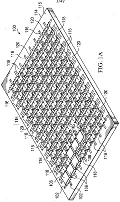
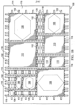
Microfluidic large scale integration
PatentInactiveUS8220494B2
Innovation
- The development of microfluidic valves using multilayer soft lithography with elastomer membrane portions of substantially constant thickness, allowing for low actuation pressures and active functions like pumps and mixers in integrated microfluidic chips, characterized by actuation pressure and flow resistance measurements across various design parameters.
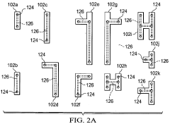
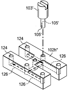
Modular microfluidic system and method for building a modular microfluidic system
PatentWO2009117147A1
Innovation
- A modular microfluidic system comprising a motherboard with channels, channel inserts, and micromodules connected via fitting components, allowing for easy assembly and reconfiguration of components to form a larger integrated system, enabling rapid customization and reducing development time and costs.
Materials Science Advancements for Microfluidic Scaling
The evolution of materials science has been pivotal in addressing the scalability challenges of microfluidic systems. Traditional materials like polydimethylsiloxane (PDMS) have dominated lab-scale applications due to their optical transparency, gas permeability, and ease of prototyping. However, these materials present significant limitations when transitioning to mass production environments, including inconsistent surface properties, limited chemical compatibility, and labor-intensive fabrication processes.
Recent advancements in thermoplastics such as cyclic olefin copolymer (COC) and polymethyl methacrylate (PMMA) have emerged as promising alternatives for large-scale manufacturing. These materials offer superior mechanical stability, reduced gas permeability, and compatibility with established industrial processes like injection molding and hot embossing, enabling production rates thousands of times faster than PDMS-based methods.
Hybrid material systems represent another frontier in microfluidic scaling. By combining the advantages of different materials—such as thermoplastic structural components with specialized functional surfaces—manufacturers can optimize both performance and production efficiency. For instance, selective surface modification techniques allow for precise control of wettability and biomolecule interactions while maintaining bulk material properties suitable for mass production.
Nanomaterials integration has revolutionized the functional capabilities of microfluidic devices. Carbon nanotubes, graphene, and metal nanoparticles incorporated into microfluidic substrates enable enhanced electrical conductivity, improved heat transfer, and novel sensing capabilities. These advancements facilitate more complex integrated systems while maintaining manufacturability through techniques like roll-to-roll processing.
Biodegradable and sustainable materials represent an emerging trend addressing environmental concerns in large-scale microfluidic production. Materials such as polylactic acid (PLA) and cellulose derivatives offer comparable performance to traditional plastics while reducing environmental impact. This shift aligns with growing regulatory pressures and corporate sustainability initiatives across the biomedical and diagnostic industries.
Surface engineering technologies have evolved to overcome interface challenges in scaled microfluidic systems. Advanced techniques like plasma treatment, chemical vapor deposition, and layer-by-layer assembly enable precise control of surface properties without compromising bulk material characteristics or manufacturing throughput. These innovations are particularly crucial for applications requiring specific cell adhesion properties or protein resistance.
The convergence of materials science with digital manufacturing technologies presents unprecedented opportunities for microfluidic scaling. Additive manufacturing with specialized biocompatible resins allows for rapid iteration and customization while maintaining consistency across production batches. This approach is particularly valuable for personalized medicine applications where device customization and production speed are equally important considerations.
Cost-Benefit Analysis of Manufacturing Technologies
The economic viability of microfluidic manufacturing technologies requires thorough cost-benefit analysis to determine optimal implementation strategies. Traditional manufacturing methods for microfluidic devices, such as soft lithography, involve significant initial capital investments in cleanroom facilities and specialized equipment, often exceeding $1-5 million for comprehensive setups. However, these methods typically result in higher per-unit costs ranging from $10-100 per device due to labor-intensive processes and limited throughput.
Emerging mass production technologies like injection molding and hot embossing present compelling alternatives with substantially different cost structures. These approaches require higher initial tooling investments ($50,000-200,000 for molds and equipment) but dramatically reduce per-unit costs to potentially under $1 when produced at volumes exceeding 10,000 units. The break-even point typically occurs between 5,000-15,000 units, depending on device complexity and material selection.
Materials selection significantly impacts both manufacturing costs and device performance. While PDMS remains dominant in research settings due to its optical clarity and gas permeability, its manual processing limits scalability. Thermoplastics like COC, PMMA, and PS offer superior mass manufacturing compatibility with 30-60% lower material costs at scale, though they may require design modifications to achieve comparable performance characteristics.
Automation integration presents another critical cost-benefit consideration. Semi-automated assembly systems require moderate capital expenditure ($200,000-500,000) but can reduce labor costs by 40-70% while improving production consistency. Fully automated systems demand substantially higher investment ($1-3 million) but can achieve 85-95% labor reduction with 24/7 operation capabilities, becoming economically justified at annual production volumes exceeding 50,000-100,000 units.
Quality control technologies represent an often underestimated cost factor. Implementing comprehensive optical inspection systems adds $100,000-300,000 to initial investments but reduces defect rates from typical 5-15% to below 1%, significantly improving yield and reducing wastage costs. The economic benefit becomes particularly pronounced for high-value applications where device failure carries substantial downstream consequences.
Sustainability considerations increasingly influence manufacturing economics. While environmentally optimized production processes may increase initial costs by 10-20%, they can yield long-term benefits through reduced waste management expenses, regulatory compliance, and market differentiation. Recyclable materials and energy-efficient manufacturing can reduce lifetime environmental impact by 30-50% compared to conventional approaches.
Unlock deeper insights with Patsnap Eureka Quick Research — get a full tech report to explore trends and direct your research. Try now!
Generate Your Research Report Instantly with AI Agent
Supercharge your innovation with Patsnap Eureka AI Agent Platform!