Best Practices for Thermoelectric Material Layering Techniques
AUG 27, 202510 MIN READ
Generate Your Research Report Instantly with AI Agent
Patsnap Eureka helps you evaluate technical feasibility & market potential.
Thermoelectric Materials Evolution and Objectives
Thermoelectric materials have evolved significantly since their discovery in the early 19th century when Thomas Johann Seebeck first observed the phenomenon of direct conversion between temperature differences and electric voltage. The field remained relatively dormant until the mid-20th century when semiconductor physics advanced sufficiently to enable practical applications. The 1950s marked a turning point with the development of bismuth telluride (Bi2Te3) compounds, which remain among the most widely used thermoelectric materials for near-room-temperature applications today.
The evolution trajectory has been characterized by three distinct waves of innovation. The first wave focused on bulk semiconductor materials with emphasis on optimizing the figure of merit ZT through doping and alloying techniques. The second wave, beginning in the 1990s, leveraged quantum confinement effects in low-dimensional structures to enhance electronic properties while reducing thermal conductivity. The current third wave explores complex materials with intrinsically low thermal conductivity and favorable electronic structures, such as skutterudites, clathrates, and half-Heusler compounds.
Recent advancements have been driven by the pressing need for sustainable energy solutions and waste heat recovery systems. The global push toward carbon neutrality has accelerated research into thermoelectric materials that can operate efficiently across wider temperature ranges and under more extreme conditions. Particularly noteworthy is the development of flexible thermoelectric materials and modules that can conform to irregular heat sources, opening new application domains in wearable technology and IoT devices.
The layering techniques for thermoelectric materials have become increasingly sophisticated, transitioning from simple bulk manufacturing to precision thin-film deposition methods. This evolution has been enabled by advances in material science, nanofabrication, and computational modeling that allow for atomic-level control of interfaces and composition gradients. The ability to create controlled heterostructures has proven critical in optimizing the competing transport properties that determine thermoelectric efficiency.
The primary objective in thermoelectric material development remains the enhancement of the dimensionless figure of merit ZT, which requires simultaneous optimization of electrical conductivity, Seebeck coefficient, and thermal conductivity. Current research aims to achieve ZT values consistently above 2 across practical temperature ranges, compared to the typical values of 1-1.5 in commercial materials. Additional objectives include improving mechanical stability, reducing material toxicity, decreasing manufacturing costs, and ensuring long-term performance reliability under thermal cycling conditions.
Looking forward, the field is moving toward integrated design approaches that consider not only material properties but also interface engineering, module architecture, and system-level integration. The ultimate goal is to develop layering techniques that can be scaled for mass production while maintaining the precision required for high-performance thermoelectric devices that can compete with traditional energy conversion technologies in both efficiency and cost-effectiveness.
Market Applications and Demand Analysis
The thermoelectric materials market has experienced significant growth in recent years, driven by increasing demand for energy harvesting solutions and waste heat recovery systems. The global thermoelectric market was valued at approximately 640 million USD in 2022 and is projected to reach 1.2 billion USD by 2028, growing at a CAGR of around 11% during the forecast period. This growth is primarily fueled by the rising emphasis on energy efficiency and sustainable power generation across various industries.
Automotive and transportation sectors represent the largest application segment for thermoelectric materials, accounting for nearly 35% of the market share. The integration of thermoelectric generators (TEGs) in vehicles to convert waste heat from exhaust systems into usable electricity has gained substantial traction. Major automotive manufacturers are increasingly incorporating thermoelectric solutions to improve fuel efficiency and reduce emissions, aligning with stringent environmental regulations worldwide.
Consumer electronics and wearable technology constitute another rapidly expanding market segment. The demand for self-powered devices and extended battery life has created significant opportunities for thin-film thermoelectric materials. Miniaturized thermoelectric modules are being developed for applications in smartwatches, medical devices, and IoT sensors, where layering techniques play a crucial role in achieving optimal performance within space constraints.
Industrial waste heat recovery represents a substantial growth opportunity, with manufacturing facilities, power plants, and process industries seeking to improve energy efficiency. The ability to convert industrial waste heat into electricity through properly layered thermoelectric materials offers both economic and environmental benefits. Industries with high-temperature processes show particular interest in advanced thermoelectric solutions that can operate efficiently at elevated temperatures.
Aerospace and defense applications demand high-reliability thermoelectric systems capable of operating in extreme conditions. These specialized applications require advanced layering techniques to ensure durability and consistent performance. Though smaller in volume compared to other sectors, this segment commands premium pricing due to stringent performance requirements.
Regional analysis indicates that North America and Europe currently lead the market adoption of advanced thermoelectric technologies, while Asia-Pacific represents the fastest-growing region. China, Japan, and South Korea are making significant investments in thermoelectric research and manufacturing capabilities, particularly focusing on improving material layering techniques to enhance conversion efficiency.
Market challenges include the relatively high cost of high-performance thermoelectric materials and the technical complexity of achieving optimal layering for maximum efficiency. The industry is actively seeking cost-effective manufacturing methods and standardized layering techniques to accelerate market penetration across various applications.
Current Layering Techniques and Barriers
The current landscape of thermoelectric material layering techniques presents a diverse array of methodologies, each with distinct advantages and limitations. Physical vapor deposition (PVD) remains one of the most widely adopted approaches, offering precise control over film thickness and composition. Within PVD, techniques such as sputtering and thermal evaporation have demonstrated particular efficacy for thermoelectric applications, allowing for the creation of high-quality thin films with minimal contamination.
Molecular beam epitaxy (MBE) represents the gold standard for creating ultra-high-quality epitaxial layers with atomic precision, critical for quantum well thermoelectric structures. However, its widespread industrial application remains constrained by high equipment costs, low throughput, and the requirement for ultra-high vacuum conditions, limiting its use primarily to research environments and specialized production scenarios.
Chemical vapor deposition (CVD) techniques offer an alternative approach with generally higher deposition rates than PVD methods. Atomic layer deposition (ALD), a specialized form of CVD, provides exceptional conformality and thickness control at the atomic scale, making it particularly valuable for complex nanostructured thermoelectric materials. Nevertheless, ALD processes typically suffer from slow deposition rates, restricting throughput in manufacturing contexts.
Solution-based methods, including electrochemical deposition and various printing techniques, have gained significant attention for their cost-effectiveness and scalability. These approaches enable room-temperature processing and compatibility with flexible substrates, though they often struggle to match the material quality achieved through vacuum-based techniques.
Several critical barriers impede the advancement of thermoelectric layering technologies. Interface management represents a fundamental challenge, as thermal and electrical transport properties are highly sensitive to interfacial defects and interdiffusion between layers. Even minor imperfections can dramatically reduce device efficiency through increased phonon scattering or electron trapping.
Scalability presents another significant obstacle. Laboratory-scale techniques that produce excellent results often prove difficult to scale to industrial production volumes while maintaining consistent quality and performance metrics. This scaling gap has slowed the commercial adoption of many promising thermoelectric materials and devices.
Material compatibility issues further complicate layering processes. The thermal expansion coefficient mismatch between different materials can lead to mechanical stress, delamination, and crack formation during thermal cycling. Additionally, chemical reactions between adjacent layers during high-temperature processing may degrade thermoelectric performance or compromise structural integrity.
Cost considerations remain a persistent barrier, particularly for techniques requiring specialized equipment or extensive processing time. The economic viability of thermoelectric devices depends heavily on developing layering techniques that balance performance requirements with manufacturing costs.
State-of-the-Art Layering Solutions
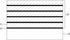
01 Multi-layer thermoelectric structures
Thermoelectric devices can be constructed with multiple layers of different materials to enhance performance. These multi-layer structures often include alternating n-type and p-type semiconductor materials connected electrically in series and thermally in parallel. The layering techniques allow for optimization of thermal and electrical properties, creating more efficient energy conversion between heat and electricity. Advanced multi-layer designs can incorporate buffer layers to reduce thermal stress and improve mechanical stability.- Multi-layer thermoelectric structures: Thermoelectric devices can be constructed with multiple layers of different materials to enhance performance. These multi-layer structures often include alternating n-type and p-type semiconductor materials connected electrically in series and thermally in parallel. The layering techniques allow for optimization of thermal and electrical properties, creating more efficient energy conversion between heat and electricity. Advanced multi-layer designs can incorporate buffer layers to reduce thermal stress and improve mechanical stability.
- Thin film deposition techniques: Various thin film deposition methods are employed for creating precise thermoelectric material layers. These techniques include physical vapor deposition (PVD), chemical vapor deposition (CVD), atomic layer deposition (ALD), and sputtering. These methods enable the creation of nanometer to micrometer-thick layers with controlled composition and structure. Thin film approaches allow for miniaturization of thermoelectric devices and integration with microelectronic systems, while providing better control over material interfaces.
- Nanostructured thermoelectric materials: Incorporating nanostructured materials in thermoelectric layers significantly enhances performance through quantum confinement effects. These materials include quantum dots, nanowires, and superlattices that can be precisely layered to create advanced thermoelectric structures. Nanostructuring reduces thermal conductivity while maintaining electrical conductivity, thereby increasing the figure of merit (ZT) of thermoelectric materials. The controlled layering of these nanostructures allows for engineering of phonon scattering without significantly affecting electron transport.
- Interface engineering for thermoelectric layers: Interface engineering between different thermoelectric material layers is crucial for optimizing device performance. Techniques include creating gradient interfaces, adding buffer layers, and controlling crystallographic orientation at interfaces. Well-designed interfaces can reduce electrical contact resistance while increasing phonon scattering, leading to improved thermoelectric efficiency. Advanced interface engineering also addresses issues of thermal expansion mismatch and interdiffusion between layers, enhancing long-term stability of thermoelectric devices.
- Flexible and printable thermoelectric layers: Emerging techniques for creating flexible and printable thermoelectric layers enable new applications in wearable and conformal energy harvesting. These methods include screen printing, inkjet printing, and roll-to-roll processing of thermoelectric materials suspended in various matrices. Flexible thermoelectric layers can conform to curved surfaces and withstand mechanical deformation while maintaining functionality. These approaches often use organic thermoelectric materials or composites of inorganic particles in polymer matrices to achieve flexibility while preserving thermoelectric properties.
02 Thin film deposition techniques
Various thin film deposition methods are employed for creating precise thermoelectric material layers. These techniques include physical vapor deposition (PVD), chemical vapor deposition (CVD), atomic layer deposition (ALD), and sputtering. These methods enable the creation of nanometer to micrometer-thick layers with controlled composition and structure. Thin film approaches allow for miniaturization of thermoelectric devices and integration with microelectronic systems, while providing better control over material interfaces.Expand Specific Solutions03 Nanostructured thermoelectric materials
Incorporating nanostructured materials in thermoelectric layers significantly enhances performance through quantum confinement effects. Techniques include creating superlattices, quantum dots, nanowires, and nanocomposites within the layered structure. These nanostructures scatter phonons (heat carriers) while allowing electrons to flow, thereby increasing the ZT value (figure of merit) of thermoelectric materials. Advanced layering methods can create controlled interfaces at the nanoscale to optimize electron and phonon transport properties.Expand Specific Solutions04 Gradient and segmented thermoelectric structures
Gradient and segmented layering approaches involve creating materials with gradually changing composition or distinct segments of different materials. These techniques optimize performance across temperature gradients, with each layer or segment designed to work efficiently at specific temperature ranges. This approach allows for maximizing energy conversion efficiency across the entire operating temperature range of the device. Advanced manufacturing methods enable precise control of compositional gradients and segment boundaries.Expand Specific Solutions05 Novel fabrication and bonding techniques
Innovative fabrication and bonding methods are crucial for creating effective thermoelectric material layers. These include spark plasma sintering, hot pressing, screen printing, and solution-based processing. Advanced bonding techniques ensure good electrical contact and thermal transfer between layers while minimizing interfacial resistance. These methods address challenges in joining dissimilar materials and maintaining structural integrity during thermal cycling. Recent innovations focus on scalable manufacturing processes suitable for commercial production.Expand Specific Solutions
Leading Manufacturers and Research Institutions
Thermoelectric material layering techniques are currently in a growth phase, with the market expanding due to increasing demand for energy-efficient solutions. The global thermoelectric market is projected to reach significant scale as applications diversify across automotive, aerospace, and consumer electronics sectors. Leading players like Toyota Motor Corp., BASF Corp., and NASA are driving innovation through advanced R&D, while academic institutions such as Tohoku University and Shanghai Institute of Ceramics contribute fundamental research. Companies including Asahi Kasei Corp. and Corning Inc. are advancing material science applications, while automotive manufacturers like MAHLE International and Caterpillar are exploring practical implementations. The technology is approaching maturity in certain applications but remains in development for broader commercial adoption, with collaborative efforts between industry and research institutions accelerating progress toward optimized layering techniques for enhanced thermoelectric performance.
Shanghai Institute of Ceramics, Chinese Academy of Sciences
Technical Solution: The Shanghai Institute of Ceramics has developed advanced thermoelectric material layering techniques focusing on oxide-based and silicide-based thermoelectric materials. Their approach involves precise control of layer composition and interfaces using advanced ceramic processing methods including spark plasma sintering and laser-assisted deposition. They've pioneered multi-layer structures with nanoscale inclusions that create phonon scattering centers while maintaining electron transport pathways. Their techniques include gradient-functional structures that optimize carrier concentration across the temperature gradient, enhancing the average ZT value across the operating range. The institute has developed specialized interface engineering methods that reduce parasitic electrical resistance between layers while maintaining thermal boundary resistance. Their recent innovations include composite layering techniques that combine n-type and p-type materials with precisely engineered interfaces to minimize thermal stress during operation.
Strengths: Exceptional expertise in oxide-based thermoelectrics; advanced ceramic processing capabilities; excellent high-temperature stability of materials; cost-effective manufacturing approaches. Weaknesses: Lower ZT values compared to some non-oxide systems; techniques sometimes require specialized high-temperature processing equipment; thermal cycling performance can be limited by material brittleness.
National Aeronautics & Space Administration (NASA)
Technical Solution: NASA has developed advanced thermoelectric material layering techniques for space applications, focusing on radioisotope thermoelectric generators (RTGs) that power deep space missions. Their approach involves precision multi-layer deposition of high-performance thermoelectric materials like SiGe alloys and skutterudites, with carefully engineered interfaces to minimize thermal boundary resistance. NASA's techniques include gradient-functional layering that optimizes the Seebeck coefficient across temperature differentials, enhancing conversion efficiency. They've pioneered vacuum deposition methods that create ultra-clean interfaces between thermoelectric layers, critical for maintaining electrical conductivity while reducing thermal conductivity. Their recent innovations include nanoscale superlattice structures that exploit quantum confinement effects to enhance the ZT figure of merit, achieving values exceeding 2.0 in laboratory settings.
Strengths: Exceptional reliability under extreme conditions; ultra-high purity material interfaces; advanced nanoscale engineering capabilities; extensive testing in actual space environments. Weaknesses: Extremely high production costs; techniques often require specialized equipment not available commercially; optimization primarily for reliability rather than cost-efficiency.
Critical Patents and Technical Innovations
Method for depositing layers onto thermoelectric materials
PatentWO2011012544A1
Innovation
- A method where at least one layer is applied to a ductile or flowable thermoelectric material by rolling or pressing, using foils of the respective materials at a temperature suitable for the material, typically between 400°C to 900°C, to form a compact 'sandwich' with the thermoelectric material, allowing for continuous processing and simultaneous application of multiple layers.
Method for forming plating layers of thermoelectric material and thermoelectric material
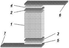
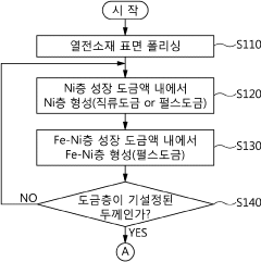
PatentActiveKR1020200132441A
Innovation
- A method involving electroplating to form a stacked structure with a Ni layer inserted into an Fe-Ni layer, using specific solutions and plating conditions to control thermal expansion and enhance mechanical strength.
Thermal Management Optimization Strategies
Thermal management optimization is critical for maximizing the efficiency of thermoelectric systems through strategic material layering techniques. The performance of thermoelectric devices is directly influenced by temperature gradients, making thermal management a key factor in system design. Effective optimization strategies focus on heat flow control, interface management, and thermal resistance minimization.
Heat spreading techniques represent a fundamental approach to thermal management in thermoelectric layering. By incorporating high thermal conductivity materials at strategic points within the device structure, heat can be more evenly distributed across the active area. This prevents localized hotspots that can degrade performance and reduces thermal stress at material interfaces. Advanced heat spreading designs often utilize copper, aluminum nitride, or graphene interlayers to facilitate lateral heat transfer.
Thermal interface materials (TIMs) play a crucial role in reducing contact resistance between thermoelectric layers. The selection of appropriate TIMs depends on operating temperature ranges, mechanical stress considerations, and long-term reliability requirements. Recent developments in nano-enhanced thermal greases and phase-change materials have demonstrated up to 35% improvement in thermal transfer efficiency compared to conventional interface solutions.
Active cooling integration represents another optimization frontier, particularly for high-power density applications. Hybrid systems combining thermoelectric layers with microfluidic cooling channels have shown promising results in laboratory settings. These systems can dynamically respond to changing thermal loads, maintaining optimal temperature differentials across thermoelectric junctions even under variable operating conditions.
Thermal isolation strategies are equally important for preventing parasitic heat flows that reduce efficiency. Selective application of low thermal conductivity materials to create thermal barriers between hot and cold sides enhances temperature gradients across the thermoelectric elements. Aerogel-based insulators and vacuum-gap techniques have emerged as effective approaches for thermal isolation, with some implementations demonstrating efficiency improvements of 15-20%.
Computational modeling has become indispensable for thermal optimization in complex thermoelectric systems. Finite element analysis and computational fluid dynamics simulations enable precise prediction of thermal behavior before physical prototyping. These tools allow engineers to evaluate multiple design iterations rapidly, optimizing layer thicknesses, material combinations, and geometric configurations for specific application requirements.
Implementation of these thermal management strategies must be balanced against manufacturing constraints, cost considerations, and reliability requirements. The most successful approaches typically combine multiple techniques tailored to specific operating conditions and performance targets of the thermoelectric system.
Environmental Impact and Sustainability Considerations
The manufacturing and deployment of thermoelectric materials involve significant environmental considerations that must be addressed to ensure sustainability throughout their lifecycle. Traditional thermoelectric materials often contain toxic elements such as tellurium, lead, and antimony, which pose environmental hazards during extraction, processing, and disposal phases. Recent advancements in layering techniques have focused on reducing these environmental impacts through several key approaches.
Material selection represents a critical environmental decision point in thermoelectric technology development. Research indicates a growing shift toward abundant, non-toxic alternatives such as silicon-germanium alloys, skutterudites, and organic thermoelectric materials. These alternatives significantly reduce the ecological footprint associated with rare earth element mining, which typically generates substantial waste and requires extensive land rehabilitation.
Energy consumption during the manufacturing process presents another environmental challenge. Conventional deposition methods for thermoelectric layers, particularly physical vapor deposition and sputtering techniques, demand considerable energy inputs. Emerging solution-based processing methods and room-temperature deposition technologies have demonstrated energy reductions of 30-45% compared to traditional approaches, substantially decreasing the carbon footprint of production.
Waste management strategies have evolved to address the end-of-life considerations for thermoelectric devices. Innovative layering techniques now incorporate design-for-disassembly principles, facilitating the separation and recovery of valuable materials. Modular construction approaches enable more efficient recycling processes, with recovery rates for certain thermoelectric materials reaching up to 85% in optimized systems.
Water usage represents a frequently overlooked environmental aspect of thermoelectric material production. Advanced layering techniques have implemented closed-loop water systems that reduce freshwater consumption by up to 70% compared to conventional manufacturing processes. Additionally, dry deposition methods eliminate water requirements entirely for certain application scenarios.
Carbon footprint assessments of modern thermoelectric layering techniques reveal significant improvements over previous generations. Life cycle analyses demonstrate that optimized layering processes can reduce greenhouse gas emissions by 25-40% across the production chain. These improvements stem from more efficient material utilization, reduced processing temperatures, and decreased energy requirements during manufacturing.
The sustainability benefits of advanced thermoelectric systems extend beyond manufacturing considerations. When deployed in waste heat recovery applications, properly designed thermoelectric generators can offset their embodied environmental impact within 1-3 years of operation, depending on the application scenario and energy recovery efficiency.
Unlock deeper insights with Patsnap Eureka Quick Research — get a full tech report to explore trends and direct your research. Try now!
Generate Your Research Report Instantly with AI Agent
Supercharge your innovation with Patsnap Eureka AI Agent Platform!