Optimize Electrical Conductance in Thermoelectric Devices
AUG 27, 202510 MIN READ
Generate Your Research Report Instantly with AI Agent
Patsnap Eureka helps you evaluate technical feasibility & market potential.
Thermoelectric Technology Background and Objectives
Thermoelectric technology has evolved significantly since its discovery in the early 19th century when Thomas Johann Seebeck first observed the conversion of temperature differences into electrical voltage. This phenomenon, known as the Seebeck effect, laid the foundation for thermoelectric materials and devices that can directly convert heat into electricity without moving parts or chemical reactions. The subsequent discovery of the Peltier effect in 1834 further expanded the potential applications by enabling the reverse process—using electricity to create temperature differences.
Over the past two decades, thermoelectric technology has gained renewed attention due to increasing global energy concerns and the push for sustainable energy solutions. The ability to harvest waste heat from industrial processes, automotive exhaust systems, and even body heat represents a significant opportunity for energy recovery and efficiency improvement. Current global energy consumption patterns indicate that approximately 60% of primary energy is wasted as heat, highlighting the enormous potential for thermoelectric energy harvesting.
The fundamental challenge in thermoelectric technology lies in optimizing the figure of merit ZT, which depends on three interdependent parameters: electrical conductivity, thermal conductivity, and Seebeck coefficient. Historically, improving one parameter often negatively impacts another, creating what researchers call the "thermoelectric trade-off." Specifically, enhancing electrical conductance typically increases thermal conductivity, which is counterproductive for thermoelectric efficiency.
Recent advancements in nanotechnology, materials science, and quantum engineering have opened new pathways to overcome these traditional limitations. Nanostructuring approaches, quantum confinement effects, and band engineering techniques have demonstrated promising results in decoupling these interdependent parameters. The emergence of novel materials such as skutterudites, clathrates, and half-Heusler alloys has pushed ZT values from the traditional 1.0 to above 2.0 in laboratory settings.
The primary technical objective in optimizing electrical conductance in thermoelectric devices is to enhance charge carrier mobility while simultaneously maintaining or reducing thermal conductivity. This requires precise control over material composition, crystal structure, and interfaces at the nanoscale. Secondary objectives include improving material stability at high temperatures, reducing manufacturing costs, and developing scalable production techniques suitable for commercial applications.
Looking forward, the field aims to achieve ZT values exceeding 3.0, which would make thermoelectric generators competitive with traditional power generation methods in certain applications. Additionally, there is growing interest in flexible thermoelectric materials for wearable electronics and IoT devices, as well as transparent thermoelectric materials for smart window applications. These emerging directions represent the frontier of thermoelectric research and development, with significant potential for technological breakthroughs in the coming decade.
Market Analysis for High-Efficiency Thermoelectric Applications
The global thermoelectric device market is experiencing significant growth, driven by increasing demand for energy-efficient solutions across multiple industries. Current market valuations place the sector at approximately $460 million in 2023, with projections indicating a compound annual growth rate (CAGR) of 8.3% through 2030, potentially reaching $790 million by the end of the decade. This growth trajectory is supported by expanding applications in automotive, aerospace, industrial, and consumer electronics sectors.
The automotive industry represents the largest market segment for high-efficiency thermoelectric applications, accounting for nearly 35% of the total market share. This dominance stems from the integration of thermoelectric generators (TEGs) in vehicle waste heat recovery systems, which can improve fuel efficiency by 3-5% in conventional vehicles and extend the range of electric vehicles by converting thermal energy from battery systems into usable electricity.
Consumer electronics constitutes the fastest-growing segment, with a projected CAGR of 10.2% through 2030. The miniaturization of thermoelectric cooling solutions for processors, sensors, and portable devices is driving this growth, as manufacturers seek more efficient thermal management solutions that can operate without moving parts.
Geographically, North America and Europe currently lead the market with combined market share exceeding 60%, primarily due to stringent energy efficiency regulations and substantial R&D investments. However, the Asia-Pacific region is expected to witness the highest growth rate, fueled by rapid industrialization in China, Japan, and South Korea, and increasing adoption of waste heat recovery technologies across manufacturing sectors.
Market analysis reveals that customers are increasingly prioritizing thermoelectric solutions with higher ZT values (figure of merit), with particular emphasis on materials and designs that optimize electrical conductance while minimizing thermal conductivity. This demand is creating premium market segments for high-efficiency devices that can achieve conversion efficiencies above 10%, compared to traditional devices operating at 5-7% efficiency.
Key market barriers include the relatively high cost of high-performance thermoelectric materials and manufacturing complexities. Current production costs for advanced thermoelectric modules range from $5-15 per watt of generating capacity, significantly higher than competing technologies. However, economies of scale and material innovations are expected to reduce these costs by 30-40% over the next five years, potentially accelerating market penetration.
The market landscape is also being shaped by emerging applications in renewable energy systems, medical devices, and space exploration, which collectively represent approximately 15% of current market value but are projected to account for over 25% by 2030. These specialized applications often demand customized thermoelectric solutions with optimized electrical conductance properties tailored to specific operating conditions.
Current Challenges in Electrical Conductance Optimization
The optimization of electrical conductance in thermoelectric devices faces several significant challenges that have hindered widespread commercial adoption despite decades of research. The fundamental physics-based trade-off between electrical conductivity and thermal conductivity, known as the Wiedemann-Franz law, creates an inherent limitation where improving electrical conductance often leads to increased thermal conductance, which reduces the overall thermoelectric efficiency.
Material-level challenges present another major obstacle. Traditional thermoelectric materials like bismuth telluride (Bi₂Te₃) and lead telluride (PbTe) exhibit limited electrical conductance optimization potential due to their intrinsic band structures. The difficulty in simultaneously achieving high carrier mobility and optimal carrier concentration creates a complex optimization problem that has not been fully resolved with conventional materials.
Interface engineering represents a critical challenge area, as contact resistance at material interfaces can significantly degrade device performance. The formation of potential barriers at these interfaces often leads to electron scattering, reducing overall electrical conductance. Current manufacturing techniques struggle to create atomically smooth interfaces that would minimize these effects.
Nanoscale engineering approaches, while promising, face scalability issues. Techniques such as quantum confinement and energy filtering can theoretically enhance electrical conductance while suppressing thermal transport, but implementing these approaches in mass-produced devices remains problematic. The precise control required for nanoscale structures is difficult to maintain in industrial manufacturing environments.
Temperature stability presents another significant challenge. Many thermoelectric materials that show promising electrical conductance at room temperature experience dramatic performance degradation at higher operating temperatures due to increased phonon scattering and carrier concentration changes. This limits their practical application in high-temperature waste heat recovery systems.
Manufacturing consistency and cost-effectiveness remain persistent obstacles. Current fabrication methods for high-performance thermoelectric materials often involve complex processes that are difficult to scale economically. The precision required for optimal electrical conductance often conflicts with mass production capabilities, creating a barrier to commercial viability.
Doping strategies, while effective for tuning electrical properties, introduce their own challenges. Achieving uniform dopant distribution throughout the material matrix is technically difficult, and dopant stability over time and temperature cycling remains problematic. These issues can lead to performance degradation and reduced device lifespan.
State-of-the-Art Electrical Conductance Solutions
01 Materials for enhancing electrical conductance in thermoelectric devices
Various materials can be incorporated into thermoelectric devices to enhance their electrical conductance. These materials include specialized semiconductors, nanostructured composites, and doped compounds that optimize the electrical properties while maintaining thermal resistance. By carefully selecting and engineering these materials, the power generation efficiency and performance of thermoelectric devices can be significantly improved.- Materials for enhancing electrical conductance in thermoelectric devices: Various materials can be incorporated into thermoelectric devices to enhance their electrical conductance while maintaining low thermal conductivity. These materials include specialized semiconductors, nanostructured composites, and doped polymers that optimize the power factor of thermoelectric devices. The improved electrical conductance leads to better energy conversion efficiency and overall device performance.
- Structural designs to improve electrical conductance: Innovative structural designs can significantly improve the electrical conductance of thermoelectric devices. These designs include multi-layered structures, segmented legs, and specialized junction configurations that reduce contact resistance. By optimizing the physical arrangement of thermoelectric components, these designs create more efficient pathways for electrical current while minimizing thermal losses.
- Integration of conductive elements in thermoelectric systems: The integration of highly conductive elements within thermoelectric systems enhances overall electrical performance. These elements include metallic interconnects, conductive adhesives, and specialized electrode materials that create low-resistance electrical pathways. Such integration techniques minimize parasitic resistance losses and improve the power output of thermoelectric generators or the cooling efficiency of thermoelectric coolers.
- Surface treatments and interface engineering: Surface treatments and interface engineering techniques are employed to enhance electrical conductance in thermoelectric devices. These include specialized coatings, surface modification processes, and interface layers that reduce contact resistance between different materials. By optimizing the interfaces between thermoelectric elements and electrical contacts, these techniques minimize energy losses and improve overall device efficiency.
- Novel manufacturing processes for conductance optimization: Advanced manufacturing processes have been developed to optimize the electrical conductance of thermoelectric devices. These include precision deposition techniques, controlled doping methods, and specialized sintering processes that enhance carrier mobility and concentration. These manufacturing innovations enable the production of thermoelectric devices with precisely tailored electrical properties and improved performance characteristics.
02 Structural designs to improve electrical conductance
Innovative structural designs can be implemented to improve the electrical conductance of thermoelectric devices. These designs include layered structures, segmented elements, and specialized junction configurations that optimize electron flow while minimizing thermal conductivity. Such structural modifications can enhance the overall efficiency and performance of thermoelectric generators and cooling systems.Expand Specific Solutions03 Integration of nanomaterials for enhanced thermoelectric performance
Nanomaterials can be integrated into thermoelectric devices to enhance their electrical conductance while reducing thermal conductivity. These include quantum dots, nanowires, and two-dimensional materials that create quantum confinement effects. The incorporation of these nanomaterials allows for selective scattering of phonons while maintaining good electron transport, thereby improving the figure of merit (ZT) of thermoelectric devices.Expand Specific Solutions04 Interface engineering for optimized electrical properties
Interface engineering techniques can be applied to optimize the electrical properties of thermoelectric devices. These techniques involve controlling the boundaries between different materials, creating specific junction characteristics, and managing contact resistances. By carefully designing and treating interfaces, electron transport can be enhanced while phonon transport is suppressed, leading to improved thermoelectric performance.Expand Specific Solutions05 Doping strategies to control carrier concentration
Various doping strategies can be employed to control carrier concentration and optimize the electrical conductance of thermoelectric materials. These include introducing specific impurities, creating controlled defects, and implementing gradient doping profiles. By precisely managing the type and concentration of carriers, the electrical conductivity can be enhanced while maintaining a high Seebeck coefficient, resulting in improved thermoelectric efficiency.Expand Specific Solutions
Leading Companies and Research Institutions in Thermoelectrics
The thermoelectric device electrical conductance optimization market is currently in a growth phase, with increasing demand driven by energy efficiency requirements across multiple sectors. The global thermoelectric market is projected to reach approximately $1.5 billion by 2027, with a CAGR of 8-10%. Technology maturity varies significantly among key players, with established companies like Toyota Motor Corp., Gentherm, and Toshiba leading commercial applications, while research institutions such as Shanghai Institute of Ceramics and Shandong University focus on fundamental breakthroughs. Companies including LG Innotek, Sony, and Samsung are advancing material science innovations to overcome the traditional conductivity-thermal conductivity trade-off. The competitive landscape features automotive manufacturers, electronics conglomerates, and specialized thermoelectric developers collaborating with research institutions to enhance device efficiency and expand applications.
Gentherm, Inc.
Technical Solution: Gentherm has pioneered a multi-faceted approach to optimizing electrical conductance in thermoelectric devices, focusing particularly on automotive and medical applications. Their technology employs advanced doping strategies for semiconductor materials, precisely controlling carrier concentration to maximize electrical conductivity while minimizing thermal conductivity. Gentherm's proprietary manufacturing process incorporates gradient-structured materials that optimize electron transport across the entire operating temperature range. Their latest generation of materials features controlled introduction of nanoscale precipitates that create energy filtering effects, allowing only high-energy carriers to contribute to electrical conduction while scattering phonons. This approach has yielded thermoelectric materials with figure of merit (ZT) values approaching 2.0 under specific operating conditions, representing a significant improvement over conventional materials with ZT values of 1.0-1.2. Gentherm has successfully integrated these advanced materials into commercial climate control systems for automotive seating and medical devices.
Strengths: Extensive real-world implementation experience in automotive applications; vertical integration from material development to system design enables holistic optimization. Weaknesses: Solutions are primarily optimized for near-room-temperature applications, limiting effectiveness in high-temperature waste heat recovery; relatively high production costs compared to conventional heating/cooling technologies.
Shanghai Institute of Ceramics, Chinese Academy of Sciences
Technical Solution: The Shanghai Institute of Ceramics (SIC-CAS) has developed groundbreaking approaches to optimizing electrical conductance in thermoelectric materials through their "phonon-glass electron-crystal" (PGEC) design paradigm. Their research focuses on complex oxide and chalcogenide materials with intrinsically low thermal conductivity but engineered for enhanced electrical properties. SIC-CAS has pioneered the development of misfit-layered cobalt oxides with natural superlattice structures that provide intrinsically high electrical conductivity along specific crystallographic directions while disrupting thermal transport. Their most advanced materials incorporate controlled introduction of nanoscale precipitates and defect structures that create energy filtering effects, allowing only high-mobility carriers to contribute to electrical conduction. This approach has yielded n-type and p-type materials with complementary performance characteristics, enabling the creation of highly efficient thermoelectric modules. Their latest generation materials demonstrate ZT values exceeding 1.5 at high temperatures (>700K), making them particularly suitable for industrial waste heat recovery applications where traditional materials suffer from stability issues.
Strengths: World-leading expertise in complex oxide thermoelectric materials that offer superior high-temperature stability; innovative approaches to decoupling electrical and thermal transport. Weaknesses: Some materials systems require precise control of oxygen stoichiometry during manufacturing, creating production challenges; relatively lower performance at room temperature compared to conventional bismuth telluride systems.
Key Patents and Breakthroughs in Conductivity Enhancement
Method for production of a thermoelectric conversion element
PatentInactiveEP2556909A1
Innovation
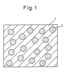
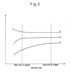
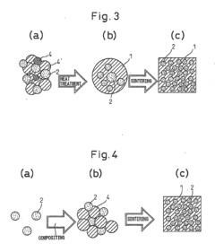
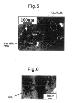
- Dispersing metal or alloy particles with an average size of 1 to 100 nm within the thermoelectric conversion material, ensuring they are positioned at a distance not exceeding the mean free path of phonons, and using a method involving solution deposition and heat treatment to form composite particles with controlled dispersion distances, thereby enhancing phonon scattering and maintaining electrical conductivity.
Thermoelectric devices having reduced parasitics
PatentInactiveUS20140305479A1
Innovation
- The proposed solution involves a thermoelectric device design with a reduced number of interfaces and optimized dimensions for thermoelectric elements and conductors, using a pi topology with spray-coated thermoelectric materials on conductive substrates to minimize parasitic resistances and enhance thermal and electrical conductivity.
Environmental Impact and Sustainability Considerations
The optimization of electrical conductance in thermoelectric devices carries significant environmental implications that must be considered within a comprehensive sustainability framework. Thermoelectric technology offers promising pathways toward more efficient energy utilization, potentially reducing fossil fuel consumption and associated greenhouse gas emissions. When electrical conductance is optimized, these devices can convert waste heat into usable electricity more efficiently, creating closed-loop energy systems in industrial processes and transportation sectors.
The materials used in thermoelectric devices present important environmental considerations. Traditional thermoelectric materials often contain toxic or rare elements such as tellurium, bismuth, and lead. The mining and processing of these elements generate substantial environmental impacts, including habitat destruction, water pollution, and energy-intensive extraction processes. Recent research focusing on electrical conductance optimization has explored more abundant and environmentally benign alternatives, including silicon-germanium alloys, skutterudites, and organic thermoelectric materials.
Life cycle assessment (LCA) studies indicate that the environmental benefits of optimized thermoelectric devices can outweigh their production impacts when deployed at scale. For instance, automotive thermoelectric generators with enhanced electrical conductance can recover 5-10% of waste heat from exhaust systems, translating to meaningful reductions in fuel consumption and emissions. However, these benefits are contingent upon extending device lifespans through improved material stability and reduced degradation rates.
Manufacturing processes for high-conductance thermoelectric materials also present environmental challenges. Nanoscale engineering techniques used to optimize electrical properties often require energy-intensive processes and specialized equipment. The environmental footprint of these manufacturing methods must be weighed against the lifetime energy savings of the resulting devices. Emerging green manufacturing approaches, including aqueous synthesis methods and reduced-temperature processing, show promise for minimizing these impacts.
End-of-life considerations represent another critical sustainability dimension. The complex material compositions of advanced thermoelectric devices can complicate recycling efforts. Developing effective recovery systems for valuable or potentially harmful elements is essential for closing material loops. Design for disassembly principles should be incorporated into device architecture to facilitate material separation and recovery, particularly for devices containing rare or toxic elements used to enhance electrical conductance.
Policy frameworks increasingly recognize the dual environmental benefits of thermoelectric technologies: energy efficiency improvements and potential reductions in cooling-related refrigerants with high global warming potential. Carbon pricing mechanisms and extended producer responsibility regulations may accelerate the adoption of optimized thermoelectric solutions while encouraging sustainable material selection and manufacturing practices.
Manufacturing Scalability and Cost Analysis
The scalability of manufacturing processes for thermoelectric devices represents a critical factor in their commercial viability. Current production methods for high-performance thermoelectric materials often involve complex, multi-step processes including powder metallurgy, hot pressing, spark plasma sintering, and precision machining. These techniques, while effective for laboratory-scale production, present significant challenges when scaled to industrial volumes. The capital expenditure required for specialized equipment such as high-temperature furnaces, vacuum systems, and precision doping facilities can range from $500,000 to several million dollars, creating substantial barriers to market entry.
Material costs constitute approximately 40-60% of total production expenses for thermoelectric devices. Bismuth telluride (Bi₂Te₃), the most commonly used material for near-room-temperature applications, contains tellurium—a relatively scarce element with fluctuating market prices ($30-100/kg in recent years). Alternative materials being explored, such as skutterudites and half-Heusler alloys, may offer better electrical conductance properties but often incorporate rare earth elements or precious metals, further increasing raw material costs.
Labor intensity presents another significant manufacturing challenge. The precise doping required to optimize electrical conductance demands highly controlled production environments and skilled technicians. Current manufacturing yields for high-performance thermoelectric modules typically range from 70-85%, with defects often occurring during the critical electrical contact formation stage. Each percentage improvement in yield can translate to approximately 1-2% reduction in overall production costs.
Economies of scale remain difficult to achieve due to the precision requirements for maintaining optimal electrical conductance. Unlike semiconductor manufacturing, which has benefited from decades of process refinement and standardization, thermoelectric device production lacks standardized fabrication protocols. Companies like Marlow Industries and Ferrotec have developed proprietary manufacturing techniques, but these remain costly at $10-30 per watt of generating capacity—significantly higher than competing energy technologies.
Recent innovations in additive manufacturing and roll-to-roll processing show promise for reducing production costs by 30-50%. These approaches enable more precise control over material composition and interfaces—critical factors for electrical conductance optimization. Additionally, automated quality control systems utilizing machine learning algorithms are beginning to improve yield rates by identifying defects earlier in the production process, potentially reducing manufacturing costs by 15-25% over the next five years.
Unlock deeper insights with Patsnap Eureka Quick Research — get a full tech report to explore trends and direct your research. Try now!
Generate Your Research Report Instantly with AI Agent
Supercharge your innovation with Patsnap Eureka AI Agent Platform!