Challenges in Scaling Transient Electronics Manufacturing.
SEP 4, 202510 MIN READ
Generate Your Research Report Instantly with AI Agent
Patsnap Eureka helps you evaluate technical feasibility & market potential.
Transient Electronics Evolution and Objectives
Transient electronics, also known as biodegradable or dissolvable electronics, represent a revolutionary paradigm shift in the electronics industry. This technology emerged in the early 2000s with pioneering work at the University of Illinois and Northwestern University, where researchers first demonstrated electronic components capable of dissolving in controlled environments. The evolution of transient electronics has been driven by increasing environmental concerns regarding electronic waste and expanding applications in biomedical fields.
The fundamental concept behind transient electronics involves designing devices that can maintain stable operation for a predetermined period before undergoing controlled degradation. This controlled lifespan represents a significant departure from conventional electronics, which are designed for durability and longevity. The technological trajectory has evolved from simple circuits with limited functionality to increasingly complex systems capable of sensing, computing, and wireless communication.
Recent advancements have focused on developing materials that balance performance with degradability. Silicon nanomembranes, magnesium conductors, silk fibroin dielectrics, and various biodegradable polymers have emerged as key building blocks. These materials enable the creation of functional electronic components that can dissolve in water or biofluids within timeframes ranging from minutes to months, depending on design parameters.
The primary objectives of transient electronics research and development center on addressing several critical challenges. First, enhancing the performance metrics of transient devices to match conventional electronics while maintaining their degradability characteristics. Second, developing scalable manufacturing processes that can transition from laboratory prototypes to commercial production. Third, extending the functional lifetime of devices while ensuring complete degradation after their intended use period.
From an application perspective, transient electronics aim to revolutionize several sectors. In healthcare, they offer potential for implantable diagnostic or therapeutic devices that eliminate the need for surgical removal. Environmental monitoring applications include sensors that can be deployed in natural settings without retrieval concerns. Consumer electronics could benefit from reduced electronic waste through intentionally short-lived components in disposable products.
The technological roadmap for transient electronics involves progressive improvements in materials science, device architecture, and manufacturing techniques. Current objectives include developing standardized testing protocols for degradation characteristics, improving encapsulation technologies for controlled lifetimes, and creating design frameworks that accommodate the unique constraints of transient systems. These efforts collectively work toward the ultimate goal of establishing transient electronics as a mainstream alternative to conventional electronic systems in appropriate application domains.
Market Analysis for Degradable Electronic Devices
The global market for degradable electronic devices is experiencing significant growth, driven by increasing environmental concerns and the expanding applications of transient electronics. Current market estimates value this sector at approximately 500 million USD in 2023, with projections indicating a compound annual growth rate (CAGR) of 18-20% over the next five years. This rapid expansion reflects the growing recognition of the environmental impact of electronic waste and the potential benefits of biodegradable alternatives.
Healthcare represents the largest market segment for transient electronics, accounting for roughly 40% of current applications. Within this sector, implantable medical devices such as temporary sensors, drug delivery systems, and dissolvable surgical aids demonstrate the highest demand. The ability of these devices to perform their function and then safely degrade within the body eliminates the need for retrieval surgeries, reducing patient risk and healthcare costs.
Environmental monitoring applications constitute the second-largest market segment at 25%, with devices designed to track ecological parameters in remote or sensitive locations before harmlessly degrading. This application is particularly valuable for wildlife conservation efforts and monitoring pollution in protected ecosystems.
Consumer electronics represents an emerging market with significant growth potential, currently at 15% of the market but expanding rapidly. Temporary electronic tags, disposable sensors for perishable goods, and short-lifecycle consumer products are driving adoption in this segment.
Regionally, North America leads the market with 38% share, followed by Europe (30%) and Asia-Pacific (25%). However, the Asia-Pacific region is expected to demonstrate the fastest growth rate due to increasing environmental regulations, expanding healthcare infrastructure, and growing manufacturing capabilities in countries like China, Japan, and South Korea.
Key market restraints include higher production costs compared to conventional electronics, with degradable components typically commanding a 30-40% premium. Performance limitations also remain a challenge, as degradable devices generally offer shorter operational lifespans and reduced functionality compared to traditional alternatives.
Customer adoption surveys indicate that 65% of potential industrial users cite cost as the primary barrier to implementation, while 45% express concerns about reliability. However, 78% acknowledge the long-term environmental benefits and 56% report willingness to adopt these technologies if performance metrics improve and costs decrease by at least 20%.
Current Manufacturing Limitations and Technical Barriers
Despite significant advancements in transient electronics technology, scaling manufacturing processes from laboratory prototypes to commercial production faces substantial technical barriers. Current manufacturing methods predominantly rely on cleanroom-based microfabrication techniques that were originally designed for conventional electronics, creating fundamental incompatibilities with transient materials. These specialized processes require expensive equipment and highly controlled environments, significantly increasing production costs and limiting accessibility.
Material inconsistency represents a critical manufacturing challenge. Transient substrates such as silk fibroin, poly(lactic-co-glycolic acid), and magnesium alloys exhibit batch-to-batch variations in dissolution rates and mechanical properties. This inconsistency complicates process standardization and quality control, resulting in unpredictable device performance and reliability issues that hinder mass production capabilities.
Integration of dissimilar materials with varying degradation mechanisms presents another significant barrier. Transient electronics typically combine biodegradable polymers, water-soluble metals, and specialized encapsulation materials—each requiring different processing conditions. The thermal and chemical incompatibilities between these materials create processing conflicts, where optimal conditions for one component may damage another, leading to compromised device functionality and reduced manufacturing yields.
Encapsulation technology remains particularly problematic for scaled production. Current methods struggle to provide uniform, defect-free protective layers that maintain device functionality while ensuring controlled degradation. Microscopic pinholes or thickness variations in encapsulation layers can lead to premature device failure or unpredictable dissolution profiles, creating reliability concerns that limit commercial viability.
Metrology and testing infrastructure for transient electronics lags significantly behind conventional electronics manufacturing. Standard testing protocols cannot adequately characterize dissolution behavior, transient performance, or biocompatibility in dynamic environments. This deficiency in quality assurance tools makes it difficult to implement statistical process control necessary for high-volume manufacturing and regulatory compliance.
The absence of specialized equipment designed specifically for transient electronics production forces manufacturers to adapt conventional tools, resulting in process inefficiencies and yield limitations. Current production lines lack automated handling systems capable of processing delicate transient materials without damage, while existing deposition and patterning equipment struggles with the unique surface properties and thermal sensitivities of biodegradable substrates.
These technical barriers collectively create a significant gap between laboratory demonstrations and commercially viable manufacturing processes, limiting the potential for transient electronics to reach broader markets and applications despite their promising technological advantages.
Existing Manufacturing Approaches and Scalability Solutions
01 Biodegradable materials for transient electronics
Biodegradable materials are essential for transient electronics that are designed to dissolve or degrade after a specific period. These materials include water-soluble polymers, silk fibroin, and certain metal alloys that can safely decompose in biological environments. The manufacturing processes for these materials need to be scaled to ensure consistent degradation rates and functional performance while the device is operational. This approach enables applications in medical implants that don't require surgical removal.- Materials and fabrication techniques for transient electronics: Various materials and fabrication techniques are employed in the manufacturing of transient electronics. These include biodegradable substrates, water-soluble conductors, and environmentally responsive components that can dissolve or degrade under specific conditions. Advanced fabrication methods such as transfer printing, additive manufacturing, and thin-film deposition enable the creation of complex transient electronic systems with controlled lifespans. These techniques allow for precise control over the degradation timeline and functional properties of the devices.
- Scaling manufacturing processes for transient electronics: Scaling up the production of transient electronics requires specialized manufacturing approaches that balance precision with volume production capabilities. This includes adapting traditional semiconductor fabrication techniques for transient materials, developing roll-to-roll processing methods for flexible substrates, and creating automated assembly systems for delicate components. These scaling strategies focus on maintaining the critical degradation properties while achieving cost-effective mass production of transient electronic devices.
- Biomedical applications of scalable transient electronics: Transient electronics offer significant advantages for biomedical applications, where temporary functionality followed by complete dissolution eliminates the need for retrieval surgeries. Manufacturing techniques for these applications focus on biocompatible materials, sterile production environments, and precise control over dissolution rates. Scaled manufacturing processes enable the production of implantable sensors, drug delivery systems, and therapeutic devices that can safely degrade within the body after completing their intended function.
- Environmental sensing and monitoring with transient electronics: Transient electronics are being developed for environmental monitoring applications where device retrieval is impractical or environmentally harmful. Manufacturing approaches for these applications focus on creating sensors that can accurately collect data before harmlessly degrading into the environment. Scaling production of these devices involves balancing sensitivity and durability during the functional period with complete degradability afterward, often utilizing green manufacturing processes to minimize environmental impact throughout the product lifecycle.
- Integration of transient electronics with conventional systems: Manufacturing processes are being developed to integrate transient components with conventional, permanent electronic systems. These hybrid approaches allow for partial degradation of specific components while maintaining the functionality of the overall system. Scaling these manufacturing techniques involves creating compatible interfaces between transient and permanent materials, developing selective dissolution methods, and ensuring reliability of the permanent components during the degradation process of transient elements.
02 Scalable fabrication techniques for transient electronic circuits
Advanced fabrication techniques are being developed to scale the manufacturing of transient electronics. These include roll-to-roll processing, transfer printing, and additive manufacturing methods that enable high-throughput production while maintaining precise control over material deposition and device architecture. These techniques allow for the creation of ultrathin, flexible electronic components that can be produced at industrial scales while preserving the transient properties required for temporary applications.Expand Specific Solutions03 Encapsulation strategies for controlled dissolution
Effective encapsulation is crucial for controlling the lifetime and dissolution rate of transient electronics. Various encapsulation strategies have been developed, including multilayer barrier films, stimuli-responsive polymers, and composite materials that protect the functional components until triggered to dissolve. Scaling these encapsulation methods requires precise control over layer thickness and uniformity to ensure predictable device lifetimes across mass-produced units.Expand Specific Solutions04 Integration of transient components with conventional electronics
Manufacturing scalability for transient electronics often requires integration with conventional, permanent electronic components. Hybrid integration approaches allow for combining dissolving elements with traditional circuits through specialized interconnects and interface materials. This enables the creation of systems where only specific components are designed to degrade while others maintain long-term functionality, expanding the application range while leveraging existing manufacturing infrastructure.Expand Specific Solutions05 Miniaturization and performance optimization for scaled production
As transient electronics move toward commercial-scale manufacturing, significant focus is placed on miniaturization and performance optimization. This includes developing high-resolution patterning techniques, improving the electrical performance of degradable conductors, and enhancing the reliability of transient semiconductor materials. These advancements enable smaller device footprints while maintaining functionality, which is essential for applications in environmental sensors, temporary medical devices, and secure electronics.Expand Specific Solutions
Leading Companies and Research Institutions in the Field
The transient electronics manufacturing landscape is currently in an early growth phase, characterized by significant R&D investment but limited mass production capabilities. The market is projected to expand rapidly, driven by applications in medical implants, environmental monitoring, and defense. Leading semiconductor giants like TSMC, Intel, and Samsung are exploring this space, leveraging their advanced fabrication expertise. Meanwhile, specialized players such as Micron Technology and GlobalFoundries are developing novel materials and processes to address key technical challenges in controlled degradation mechanisms. Research institutions including Tsinghua University and Rochester Institute of Technology are collaborating with industry partners to overcome scalability issues related to material compatibility, manufacturing consistency, and reliability testing. The technology remains at TRL 4-6, with commercialization expected to accelerate within 3-5 years as manufacturing processes mature.
Taiwan Semiconductor Manufacturing Co., Ltd.
Technical Solution: TSMC has developed a specialized manufacturing process for transient electronics that combines biodegradable substrates with their advanced semiconductor fabrication techniques. Their approach utilizes water-soluble metals like magnesium, zinc, and iron as conductors, and silicon nanomembranes as semiconductors, all mounted on silk fibroin or poly(lactic-co-glycolic acid) (PLGA) substrates. TSMC has implemented controlled degradation mechanisms through encapsulation layers with precisely engineered dissolution rates, allowing for programmed device lifetimes ranging from days to months. Their manufacturing process incorporates specialized lithography techniques adapted for these unusual material combinations, with modified etching processes that maintain structural integrity while enabling eventual decomposition. TSMC has also developed specialized testing protocols to verify both functionality during the operational period and complete dissolution afterward[1][3].
Strengths: TSMC's advanced fabrication capabilities allow for high-precision transient devices with reliable performance during their intended lifetime. Their established manufacturing infrastructure enables potential scaling to commercial volumes. Weaknesses: The specialized materials and processes significantly increase production costs compared to conventional electronics, and the technology still faces challenges with achieving consistent dissolution rates across different environmental conditions.
Intel Corp.
Technical Solution: Intel has pioneered a platform technology for transient electronics focusing on programmable dissolution through triggered mechanisms. Their approach utilizes specialized silicon-on-insulator (SOI) technology with ultra-thin device layers that can be triggered to dissolve through electrochemical processes. Intel's manufacturing solution incorporates specialized doping profiles and material interfaces designed to facilitate controlled degradation when exposed to specific environmental triggers. The company has developed custom fabrication equipment that handles these sensitive materials while maintaining clean room compatibility. Their process integrates conventional CMOS fabrication steps with novel deposition techniques for biodegradable encapsulants and substrates. Intel has particularly focused on addressing thermal management challenges during manufacturing, as many transient materials have lower thermal stability than conventional semiconductor materials. Their approach includes specialized low-temperature processing and targeted energy delivery systems to enable precise patterning without compromising material integrity[2][5].
Strengths: Intel's approach offers precise control over dissolution timing through active triggering mechanisms, and their integration with conventional CMOS processes provides a pathway to complex functionality in transient devices. Weaknesses: The specialized equipment requirements create significant barriers to mass production, and the reliance on active triggering mechanisms adds complexity to both manufacturing and deployment.
Key Patents and Innovations in Transient Electronics Production
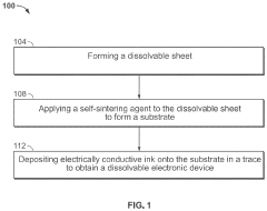
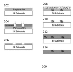
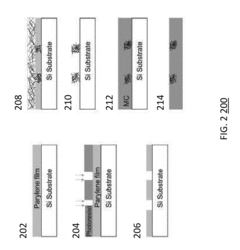
Method of manufacturing transient electronics
PatentPendingUS20240080991A1
Innovation
- The development of transient electronic devices that can chemically or physically dissolve, disintegrate, or degrade over time, using methods such as additive manufacturing to create dissolvable sheets with self-sintering agents and electrically conductive ink, or by integrating conductive materials into meltable or edible mediums, allowing for controlled end-of-life processes.
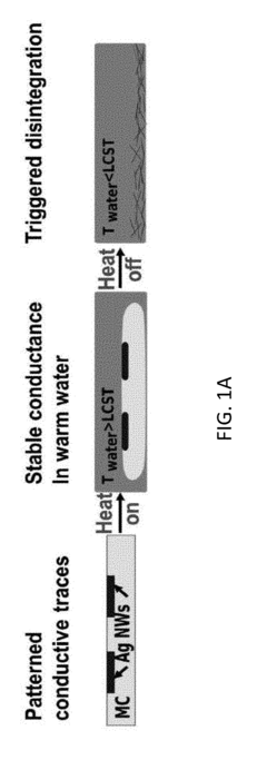
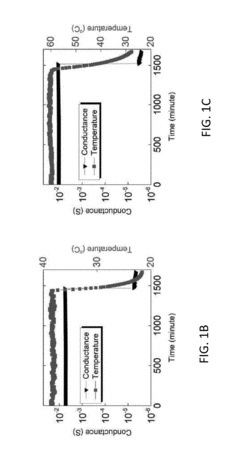
Transient electronics using thermoresponsive materials
PatentActiveUS20180174976A1
Innovation
- Employing thermoresponsive materials with lower critical solution temperature (LCST) behavior, such as methyl cellulose and poly(N-isopropylacrylamide) polymers combined with silver nanowires, to create composite elements where electrical traces are embedded or surface-disposed within a binder material, enabling stable function in warm environments and rapid disintegration upon cooling.
Environmental Impact and Sustainability Considerations
The environmental implications of transient electronics manufacturing represent a critical dimension that must be addressed as the industry scales. Conventional electronics contribute significantly to global e-waste, with approximately 50 million metric tons generated annually. Transient electronics, designed to harmlessly degrade after their functional lifetime, offer a promising alternative to this growing environmental crisis. However, the manufacturing processes themselves present several sustainability challenges that require careful consideration.
Material selection constitutes a primary environmental concern in scaling transient electronics production. While biodegradable substrates like silk fibroin and cellulose derivatives demonstrate excellent environmental compatibility, their sourcing must be managed sustainably to prevent ecosystem disruption. Additionally, certain functional components still rely on rare earth elements and potentially toxic materials that require responsible sourcing and handling protocols to minimize environmental impact.
Manufacturing processes for transient electronics currently consume substantial energy and water resources. Life cycle assessments indicate that production energy requirements can be 30-40% higher than conventional electronics due to specialized processing conditions. As scaling occurs, implementing energy-efficient manufacturing technologies and renewable energy sources becomes imperative to reduce the carbon footprint associated with production.
Chemical processing represents another significant environmental consideration. The etching solutions, solvents, and specialized chemicals used in fabrication may pose ecological risks if improperly managed. Developing green chemistry alternatives and closed-loop recycling systems for these substances will be essential for sustainable scaling of manufacturing operations.
End-of-life management, while inherently improved through transience, still presents challenges. The controlled degradation of these devices may release trace amounts of materials into ecosystems. Comprehensive testing protocols must be established to ensure that degradation byproducts do not accumulate in soil or water systems, potentially causing long-term environmental harm.
Regulatory frameworks currently lag behind the rapid development of transient electronics technology. Establishing industry-wide sustainability standards and certification processes will be crucial for ensuring environmental responsibility as manufacturing scales. These frameworks should address material sourcing, production processes, and end-of-life management to create a holistic approach to environmental stewardship.
Economic incentives for sustainable manufacturing practices will ultimately drive industry-wide adoption. Developing cost-effective green manufacturing processes that reduce resource consumption while maintaining product performance will be essential for balancing environmental considerations with commercial viability as the industry expands.
Regulatory Framework for Biodegradable Electronics
The regulatory landscape for biodegradable electronics represents a complex and evolving framework that significantly impacts the scaling of transient electronics manufacturing. Currently, there is no unified global regulatory approach specifically addressing biodegradable electronic devices, creating substantial challenges for manufacturers attempting to scale production across multiple markets.
In the United States, the FDA has begun developing preliminary guidelines for implantable biodegradable electronic devices, focusing primarily on biocompatibility testing protocols and degradation pathway verification. These guidelines, while still in development, require manufacturers to demonstrate that degradation byproducts remain below toxicity thresholds in biological systems. The EPA has also expressed interest in establishing end-of-life standards for consumer-grade transient electronics, particularly addressing concerns about potential environmental impacts of partially degraded electronic components.
The European Union has taken a more comprehensive approach through its Waste Electrical and Electronic Equipment (WEEE) Directive framework, which is being adapted to include provisions for biodegradable electronics. The European Chemicals Agency (ECHA) is currently developing specific registration requirements for novel biodegradable materials used in electronic applications, with particular emphasis on REACH compliance for degradation products.
In Asia, Japan has pioneered certification standards for biodegradable electronic components through its Eco-Mark program, while China has incorporated biodegradable electronics into its broader "green manufacturing" regulatory initiatives. South Korea has established a specialized regulatory pathway for medical biodegradable electronics through its Ministry of Food and Drug Safety.
International standards organizations, including ISO and IEC, are working to develop testing protocols and classification systems specifically for transient electronics. The IEC Technical Committee 119 has established a working group focused on standardizing terminology, testing methodologies, and performance metrics for biodegradable electronic components.
A significant regulatory challenge remains in harmonizing the diverse approaches across different jurisdictions and application domains. Medical applications face stringent biocompatibility requirements, while consumer electronics must address environmental safety concerns. This regulatory fragmentation creates substantial compliance costs that currently impede scaling efforts, as manufacturers must navigate multiple, sometimes contradictory, regulatory frameworks.
Future regulatory developments will likely focus on establishing standardized degradation testing protocols, creating unified classification systems for biodegradable electronic materials, and developing international consensus on acceptable degradation pathways and byproducts. These developments will be crucial in enabling the transition from laboratory-scale production to commercially viable manufacturing scales.
Unlock deeper insights with Patsnap Eureka Quick Research — get a full tech report to explore trends and direct your research. Try now!
Generate Your Research Report Instantly with AI Agent
Supercharge your innovation with Patsnap Eureka AI Agent Platform!