Cold Plasma Treatment Applications in Microelectronics Manufacturing
OCT 10, 202510 MIN READ
Generate Your Research Report Instantly with AI Agent
PatSnap Eureka helps you evaluate technical feasibility & market potential.
Cold Plasma Technology Evolution and Objectives
Cold plasma technology has evolved significantly since its inception in the early 20th century. Initially developed for laboratory research purposes, cold plasma applications have expanded dramatically across various industries, with microelectronics manufacturing becoming one of its most critical application domains. The fundamental principle of cold plasma—creating an ionized gas at near-ambient temperatures—has remained consistent, while the methods of generation, control, and application have undergone substantial refinement.
The 1970s marked a pivotal turning point when cold plasma began to be systematically applied in semiconductor fabrication, primarily for etching processes. This period saw the development of the first radio frequency (RF) plasma systems specifically designed for microelectronics applications. By the 1980s, plasma-enhanced chemical vapor deposition (PECVD) emerged as a groundbreaking technique, enabling the deposition of thin films at significantly lower temperatures than conventional thermal processes.
The 1990s witnessed the miniaturization revolution in microelectronics, driving the need for more precise plasma treatments. This era saw the development of high-density plasma sources, including inductively coupled plasma (ICP) and electron cyclotron resonance (ECR) systems, which offered better control over plasma parameters and reduced damage to sensitive electronic components.
The early 2000s brought atmospheric pressure plasma technologies to the forefront, eliminating the need for vacuum systems in certain applications and significantly reducing processing costs. Concurrently, pulsed plasma systems emerged, offering enhanced selectivity and reduced substrate damage through temporal control of plasma characteristics.
Current technological objectives in cold plasma applications for microelectronics manufacturing focus on several key areas. First is the development of ultra-precise plasma etching techniques capable of achieving feature sizes below 5nm, essential for advancing semiconductor node technology. Second is the integration of plasma processes with atomic layer precision for next-generation devices. Third is the creation of environmentally sustainable plasma systems that reduce greenhouse gas emissions and energy consumption.
Looking forward, the industry aims to develop intelligent plasma systems incorporating real-time monitoring and artificial intelligence for process optimization. Another objective is to expand cold plasma applications to emerging microelectronics fields, including flexible electronics, organic semiconductors, and quantum computing components, where traditional high-temperature processes are not viable.
The convergence of cold plasma technology with other advanced manufacturing techniques, such as 3D printing and roll-to-roll processing, represents another frontier, potentially enabling novel device architectures and more efficient production methodologies for next-generation microelectronic devices.
Market Analysis for Plasma Processing in Microelectronics
The global market for plasma processing in microelectronics manufacturing has experienced substantial growth over the past decade, reaching approximately $12.3 billion in 2022 with projections to exceed $18 billion by 2027, representing a compound annual growth rate (CAGR) of 7.8%. Cold plasma treatment specifically has emerged as a critical segment within this market due to its versatility and effectiveness in various microelectronics applications.
The semiconductor industry remains the primary driver of demand, accounting for nearly 65% of plasma processing equipment sales. This dominance is attributed to the continuous miniaturization of electronic components and the increasing complexity of integrated circuits, which require more precise and sophisticated manufacturing processes. Cold plasma technologies are particularly valuable in this context for their ability to perform surface modifications without thermal damage to sensitive components.
Regional analysis reveals that Asia-Pacific dominates the market with approximately 58% share, led by manufacturing powerhouses such as Taiwan, South Korea, and China. North America follows with 22% market share, while Europe accounts for 15%. The remaining 5% is distributed across other regions. This distribution closely mirrors the global semiconductor manufacturing landscape.
Market segmentation by application shows that etching processes constitute the largest segment (42%), followed by deposition (28%), cleaning (18%), and surface modification (12%). Cold plasma treatment is gaining particular traction in the cleaning and surface modification segments due to its environmental advantages over traditional chemical processes.
Consumer electronics represents the largest end-user segment (37%), followed by telecommunications (24%), automotive electronics (18%), medical devices (12%), and others (9%). The rapid expansion of IoT devices and 5G infrastructure is creating new growth opportunities for plasma processing technologies across these segments.
Key market drivers include the increasing demand for miniaturized electronic components, growing adoption of 3D integrated circuits, rising focus on environmentally friendly manufacturing processes, and the expansion of applications in emerging technologies such as flexible electronics and quantum computing. Cold plasma's ability to provide precise surface treatments while minimizing environmental impact positions it favorably within these trends.
Market challenges include high initial equipment costs, technical complexity requiring specialized expertise, integration challenges with existing manufacturing lines, and competition from alternative technologies in certain application niches. Additionally, supply chain disruptions following the COVID-19 pandemic continue to impact equipment availability and pricing.
The market is characterized by moderate concentration, with the top five players accounting for approximately 45% of the global market share. However, increasing competition from emerging Asian manufacturers is gradually reshaping the competitive landscape, particularly in mid-range equipment segments.
Current Cold Plasma Applications and Technical Barriers
Cold plasma technology has emerged as a critical process in microelectronics manufacturing, offering unique advantages for surface modification, cleaning, etching, and deposition processes. Currently, the most widespread applications include plasma etching for pattern transfer in semiconductor fabrication, where reactive ion etching (RIE) and deep reactive ion etching (DRIE) enable the creation of high-aspect-ratio structures with nanometer precision. These processes are fundamental to modern integrated circuit production, allowing manufacturers to achieve increasingly smaller feature sizes.
Surface activation and modification represent another significant application area, where cold plasma treatments alter surface energy and chemical composition to enhance adhesion properties for subsequent deposition processes. This is particularly valuable for advanced packaging technologies and heterogeneous integration, where dissimilar materials must form reliable interfaces.
Plasma-enhanced chemical vapor deposition (PECVD) has become standard for depositing thin films at lower temperatures than conventional thermal CVD processes. This enables the deposition of high-quality dielectric layers, passivation films, and barrier coatings without subjecting temperature-sensitive components to thermal damage, which is increasingly important as device architectures incorporate more thermally vulnerable materials.
Despite these successful implementations, several technical barriers limit broader adoption and advancement of cold plasma technologies in microelectronics. Plasma-induced damage remains a significant challenge, particularly for advanced semiconductor devices with nanoscale features and ultrathin gate dielectrics. Charged particles and UV radiation generated during plasma processing can create defects in sensitive materials, leading to device performance degradation.
Process uniformity across large substrates presents another major hurdle, especially as the industry transitions to larger wafer sizes. Achieving consistent plasma characteristics over 300mm or 450mm wafers requires sophisticated engineering of plasma sources and chamber designs to ensure homogeneous treatment across the entire surface.
Control precision represents a persistent challenge, as plasma processes involve complex interactions between multiple parameters including power, pressure, gas composition, and treatment duration. The interdependence of these variables makes precise process control difficult, often requiring extensive empirical optimization rather than predictive modeling.
Additionally, integration challenges arise when incorporating plasma processes into complex manufacturing flows. Compatibility with upstream and downstream processes, throughput limitations, and equipment reliability affect overall production efficiency. As devices become more complex with 3D architectures and heterogeneous integration, these integration challenges become increasingly significant.
Environmental and safety concerns also present barriers, as many plasma processes utilize greenhouse gases or toxic precursors. Developing more environmentally friendly plasma processes while maintaining performance remains an active area of research and development in the industry.
Mainstream Cold Plasma Processing Solutions
01 Medical applications of cold plasma treatment
Cold plasma technology is being utilized in various medical applications for treatment of wounds, infections, and other medical conditions. The non-thermal plasma can effectively kill bacteria and promote tissue healing without causing damage to surrounding healthy tissues. This technology is particularly useful in treating chronic wounds, dermatological conditions, and for sterilization of medical equipment.- Medical applications of cold plasma treatment: Cold plasma technology is being utilized in various medical applications for treatment of tissues and wounds. The non-thermal plasma can effectively kill bacteria and promote healing without damaging surrounding healthy tissue. These treatments can be applied to chronic wounds, dermatological conditions, and even in surgical settings where precision is required. The controlled application of cold plasma allows for targeted therapy with minimal side effects.
- Cold plasma devices and delivery systems: Various devices and systems have been developed for the effective delivery of cold plasma treatments. These include handheld applicators, specialized nozzles, and integrated treatment systems that can generate and apply cold plasma to specific areas. The designs focus on controlling plasma parameters such as temperature, gas composition, and energy levels to ensure optimal treatment outcomes while maintaining safety for both operators and patients.
- Industrial and agricultural applications of cold plasma: Cold plasma technology extends beyond medical applications into industrial and agricultural sectors. It is used for surface modification of materials, sterilization of equipment, food preservation, and seed treatment. In agriculture, cold plasma can enhance seed germination rates and plant growth while reducing pathogen loads. Industrial applications include modifying surface properties of materials to improve adhesion, wettability, or biocompatibility.
- Plasma generation methods and gas compositions: Different methods for generating cold plasma and various gas compositions significantly impact treatment efficacy. Techniques include dielectric barrier discharge, atmospheric pressure plasma jets, and microwave-induced plasma. The choice of gas (such as helium, argon, air, or nitrogen) and additives influences the reactive species produced and thus the biological effects. These parameters can be optimized for specific applications, whether for antimicrobial effects, surface modification, or tissue regeneration.
- Combination therapies with cold plasma: Cold plasma treatments are being combined with other therapeutic approaches to enhance overall efficacy. These combination therapies may include plasma treatment alongside pharmaceutical agents, photodynamic therapy, or conventional wound care protocols. The synergistic effects can lead to improved outcomes in treating resistant infections, accelerating tissue regeneration, or addressing complex medical conditions that do not respond well to single-modality treatments.
02 Cold plasma devices for therapeutic use
Various devices have been developed specifically for delivering cold plasma treatment in therapeutic settings. These devices are designed to generate controlled plasma discharges at atmospheric pressure and ambient temperature, making them suitable for direct application to biological tissues. The designs include handheld applicators, plasma jets, and specialized treatment chambers that can deliver precise doses of plasma to target areas.Expand Specific Solutions03 Surface modification and material treatment using cold plasma
Cold plasma technology is employed for surface modification of various materials including polymers, textiles, and biomaterials. The treatment can alter surface properties such as wettability, adhesion, and biocompatibility without affecting the bulk properties of the material. This has applications in manufacturing, electronics, and development of advanced materials with specific surface characteristics.Expand Specific Solutions04 Agricultural and food industry applications
Cold plasma treatment is being utilized in agriculture and food processing for decontamination, seed treatment, and shelf-life extension of food products. The technology can effectively inactivate pathogens, fungi, and pests on seeds, plants, and food surfaces without using chemicals or leaving residues. This provides an environmentally friendly alternative to traditional methods of food preservation and agricultural pest control.Expand Specific Solutions05 Environmental and industrial applications
Cold plasma technology is applied in environmental remediation and industrial processes such as wastewater treatment, air purification, and surface cleaning. The reactive species generated in plasma can break down pollutants, organic compounds, and contaminants efficiently. These applications leverage the ability of cold plasma to generate highly reactive species at low temperatures, making it energy-efficient and suitable for treating heat-sensitive materials.Expand Specific Solutions
Leading Companies in Cold Plasma Technology
Cold plasma treatment in microelectronics manufacturing is currently in a growth phase, with the market expected to reach significant expansion due to increasing demand for advanced semiconductor fabrication processes. The global market size is projected to grow substantially as miniaturization trends continue in electronics. Technologically, the field shows varying maturity levels across applications, with companies like Tokyo Electron, NAURA Microelectronics, and Advanced Micro Fabrication Equipment leading innovation in plasma etching and deposition systems. Mattson Technology and Beijing E-Town Semiconductor are advancing thermal processing applications, while research institutions like Tohoku University and Fudan University are developing next-generation plasma techniques. The competitive landscape features established equipment manufacturers alongside specialized plasma technology developers like Plasmology4, creating a dynamic ecosystem driving continuous innovation in semiconductor processing.
Tokyo Electron Ltd.
Technical Solution: Tokyo Electron (TEL) has developed advanced cold plasma treatment systems specifically for microelectronics manufacturing. Their Tactras™ platform utilizes low-temperature plasma processing for critical semiconductor fabrication steps including etching, deposition, and surface modification. The system employs capacitively coupled plasma (CCP) technology operating at temperatures below 100°C, which enables precise control of ion energy and radical density for nanoscale feature processing[1]. TEL's cold plasma solutions incorporate multi-frequency power delivery systems that allow independent control of plasma density and ion energy, critical for processing increasingly complex 3D structures in advanced node semiconductors[3]. Their systems achieve etch selectivity ratios exceeding 100:1 for certain material combinations while maintaining damage-free interfaces. TEL has also pioneered plasma-assisted atomic layer deposition (PA-ALD) techniques that utilize sequential self-limiting reactions enhanced by cold plasma to deposit ultra-thin conformal films with thickness control at the atomic level[5].
Strengths: Industry-leading plasma uniformity across 300mm wafers (<±1.5%), enabling consistent processing for advanced nodes. Proprietary endpoint detection systems that minimize over-processing and substrate damage. Weaknesses: Higher capital equipment costs compared to conventional thermal processing tools, and some processes require specialized precursors with limited suppliers.
Plasmology4, Inc.
Technical Solution: Plasmology4 has developed proprietary atmospheric pressure cold plasma technology specifically tailored for microelectronics applications. Their patented PlasmaWrap™ system generates non-thermal plasma at atmospheric pressure, eliminating the need for vacuum chambers and reducing processing complexity[2]. This technology utilizes dielectric barrier discharge (DBD) principles to create highly reactive plasma species while maintaining substrate temperatures below 50°C. The company's approach enables selective surface modification of polymers and metals used in microelectronic packaging without thermal damage to heat-sensitive components[4]. Their systems incorporate precision gas delivery with digital flow control that can adjust plasma chemistry in real-time based on feedback from integrated optical emission spectroscopy sensors. Plasmology4's technology has demonstrated particular effectiveness in improving adhesion properties for advanced packaging applications, achieving up to 300% improvement in adhesion strength for certain polymer-metal interfaces while maintaining treatment times under 30 seconds per wafer[7].
Strengths: Atmospheric pressure operation eliminates vacuum equipment requirements, reducing system footprint and capital costs. Rapid processing capabilities with treatment times typically under 30 seconds. Weaknesses: Limited penetration into high-aspect-ratio features compared to vacuum-based plasma systems, and relatively new technology with less established process recipes compared to industry incumbents.
Key Patents and Innovations in Cold Plasma Treatment
Plasma processing apparatus and method for plasma processing semiconductor substrate
PatentWO2009063755A1
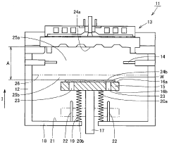
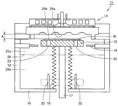
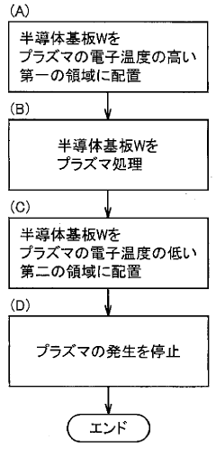
Innovation
- A plasma processing apparatus and method utilizing microwaves to create distinct regions within the chamber, positioning the substrate in a high-electron-temperature region for efficient processing and then moving it to a low-electron-temperature region to minimize charge-up damage by controlling pressure and substrate movement.
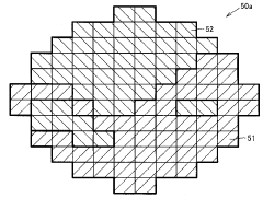
Cold plasma generating apparatus and multi-cold plasma array apparatus comprising the same
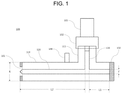
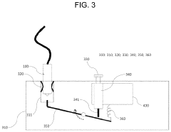
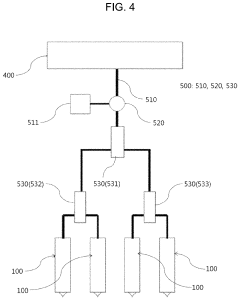
PatentActiveUS20210233746A1
Innovation
- A cold plasma generating apparatus with a cylindrical housing, central conductive center, microwave transmission member, and impedance matching adjustment member, which allows for efficient microwave transmission and impedance matching, enabling efficient plasma ignition and uniform power distribution to multiple plasma sources through a single power supply.

Environmental Impact and Sustainability Considerations
Cold plasma treatment in microelectronics manufacturing offers significant environmental advantages compared to traditional wet chemical processes. The technology substantially reduces hazardous chemical usage, with plasma processes typically consuming 80-90% fewer chemicals than conventional methods. This reduction directly translates to decreased toxic waste generation and lower environmental contamination risks associated with manufacturing operations.
Water conservation represents another critical environmental benefit of cold plasma applications. While traditional semiconductor cleaning and etching processes may require up to 1,000 liters of ultra-pure water per wafer, plasma-based alternatives can operate as essentially dry processes. This dramatic reduction in water consumption is particularly valuable as the electronics industry faces increasing scrutiny over its water footprint in water-stressed regions.
Energy efficiency considerations also favor cold plasma technologies. Modern atmospheric pressure plasma systems operate at significantly lower temperatures than thermal processes, reducing energy requirements by 30-50% in many applications. Additionally, the precise nature of plasma treatments minimizes material waste through targeted surface modifications rather than bulk material processing, contributing to resource conservation across the supply chain.
From a lifecycle perspective, cold plasma equipment demonstrates favorable sustainability metrics. The extended operational lifespan of plasma systems—typically 8-10 years with proper maintenance—reduces manufacturing infrastructure turnover. Furthermore, the elimination of many hazardous chemicals simplifies regulatory compliance and reduces costs associated with specialized handling, storage, and disposal protocols.
Looking forward, the integration of renewable energy sources with plasma systems presents promising opportunities for further reducing the carbon footprint of microelectronics manufacturing. Several leading fabrication facilities have begun implementing solar-powered plasma treatment units, demonstrating the technology's compatibility with clean energy transitions.
Despite these advantages, challenges remain in fully optimizing cold plasma's environmental profile. Certain plasma processes still utilize perfluorinated compounds with high global warming potential. Industry research is actively developing alternative process gases with reduced environmental impact while maintaining technical performance. Additionally, comprehensive lifecycle assessment methodologies specific to plasma manufacturing technologies are needed to accurately quantify their total environmental footprint compared to conventional approaches.
The semiconductor industry's roadmap increasingly emphasizes sustainability metrics alongside performance parameters, positioning environmentally advantageous technologies like cold plasma treatment as strategic priorities for future manufacturing development. This alignment between technical capabilities and sustainability goals will likely accelerate adoption across the microelectronics sector.
Integration with Advanced Manufacturing Processes
Cold plasma treatment technology has reached a critical integration point with advanced manufacturing processes in microelectronics production. The seamless incorporation of plasma treatments into existing semiconductor fabrication lines represents a significant advancement in manufacturing efficiency. Modern fabs are implementing in-line plasma cleaning and surface modification stations that operate at atmospheric pressure, eliminating the need for separate vacuum chambers and reducing production bottlenecks. This integration allows for continuous processing without breaking the production flow.
Industry 4.0 principles are being applied to plasma treatment systems through sophisticated sensor networks that enable real-time monitoring and adjustment of plasma parameters. These smart systems can detect subtle changes in surface properties and automatically modify treatment conditions to maintain consistent quality across production batches. The integration of artificial intelligence algorithms further enhances process control by predicting optimal treatment parameters based on incoming material characteristics and desired outcomes.
Roll-to-roll (R2R) manufacturing processes have successfully incorporated cold plasma treatments for flexible electronics production. These systems allow continuous treatment of polymer substrates at speeds exceeding 100 meters per minute while maintaining uniform plasma exposure. The development of specialized electrode designs for R2R systems has overcome previous limitations in treating three-dimensional features on flexible substrates.
Cluster tool architectures now commonly include dedicated plasma treatment modules alongside deposition and etching chambers. This configuration enables wafers to receive surface preparation, modification, or cleaning treatments without exposure to atmospheric contaminants between process steps. Advanced robotic handling systems coordinate the movement of substrates between modules with precision timing to optimize throughput while maintaining the benefits of plasma-prepared surfaces.
The miniaturization of plasma generation equipment has enabled integration directly into pick-and-place machinery for component-level treatments immediately before assembly. This point-of-use application ensures optimal surface conditions at the critical moment of component bonding or interconnection. Similarly, selective plasma treatment capabilities have been developed using precisely controlled plasma jets that can target specific regions of a device without affecting adjacent sensitive components.
Compatibility with cleanroom environments has been enhanced through the development of emission-controlled plasma systems that minimize particulate generation and chemical contamination. These systems employ advanced filtration and closed-loop gas handling to maintain Class 10 or better cleanroom conditions while operating. Material handling automation has evolved to accommodate plasma treatment steps with minimal human intervention, reducing contamination risks and improving process repeatability.
Unlock deeper insights with PatSnap Eureka Quick Research — get a full tech report to explore trends and direct your research. Try now!
Generate Your Research Report Instantly with AI Agent
Supercharge your innovation with PatSnap Eureka AI Agent Platform!