Cold Plasma Treatment's Effect on Semiconductor Carrier Transport
OCT 10, 20259 MIN READ
Generate Your Research Report Instantly with AI Agent
Patsnap Eureka helps you evaluate technical feasibility & market potential.
Cold Plasma Technology Evolution and Objectives
Cold plasma technology has evolved significantly over the past several decades, transitioning from a niche scientific curiosity to a versatile tool with applications across multiple industries. The journey began in the early 20th century with fundamental research on gas discharges, but it wasn't until the 1970s that researchers started exploring cold plasma's potential in materials processing. By the 1990s, semiconductor manufacturers had begun implementing plasma-based processes for etching and deposition, marking a pivotal moment in the technology's evolution.
The development trajectory accelerated in the early 2000s when researchers discovered that cold plasma treatment could significantly alter the surface properties of semiconductors without causing thermal damage to the underlying substrate. This breakthrough opened new avenues for semiconductor engineering, particularly in modifying carrier transport characteristics—a critical factor in device performance.
Recent advancements have focused on precision control of plasma parameters, including electron temperature, ion density, and reactive species composition. These refinements have enabled increasingly targeted modifications to semiconductor carrier mobility and concentration, allowing engineers to fine-tune electronic properties with unprecedented precision. The introduction of atmospheric pressure plasma systems has further expanded the technology's accessibility and application range, eliminating the need for complex vacuum systems in many processes.
The primary objective of cold plasma treatment in semiconductor applications is to enhance carrier transport properties without introducing thermal stress or structural damage. This includes increasing carrier mobility, optimizing carrier concentration, reducing interface trapping, and improving overall device efficiency. Secondary objectives include developing scalable processes suitable for industrial implementation, ensuring treatment uniformity across large wafer sizes, and maintaining process stability over extended production runs.
Looking forward, the field aims to establish comprehensive models correlating plasma parameters with resulting semiconductor properties, enabling predictive engineering of electronic characteristics. There is also significant interest in developing selective plasma treatments capable of creating spatially varied carrier transport properties within a single device—a capability that could revolutionize next-generation semiconductor design.
The convergence of cold plasma technology with emerging semiconductor materials, such as wide-bandgap semiconductors and 2D materials, represents another critical objective. Researchers are actively exploring how plasma treatments can address the unique challenges these materials present while leveraging their exceptional electronic properties for advanced applications in power electronics, optoelectronics, and quantum computing.
Semiconductor Industry Demand for Plasma Processing
The semiconductor industry's demand for plasma processing has experienced exponential growth over the past decade, driven primarily by the continuous miniaturization of electronic components and the increasing complexity of integrated circuits. Plasma processing technologies have become indispensable in modern semiconductor manufacturing, with applications spanning etching, deposition, cleaning, and surface modification processes.
Market analysis indicates that the global semiconductor plasma equipment market reached approximately $15 billion in 2022, with projections suggesting growth to $25 billion by 2027, representing a compound annual growth rate of 10.8%. This robust growth trajectory underscores the critical importance of plasma technologies in meeting the semiconductor industry's evolving requirements.
The demand for plasma processing is particularly pronounced in advanced node manufacturing, where feature sizes continue to shrink below 5nm. At these dimensions, conventional wet chemical processes face significant limitations in achieving the required precision and uniformity. Cold plasma treatments offer superior control over surface properties and can be precisely tuned to modify carrier transport characteristics without causing thermal damage to sensitive semiconductor materials.
Industry surveys reveal that 87% of semiconductor manufacturers consider plasma processing technologies essential for their future production capabilities. The ability of cold plasma to enhance carrier mobility while minimizing surface defects has become a key differentiator in high-performance semiconductor device manufacturing. This is especially relevant for emerging applications in quantum computing, neuromorphic chips, and ultra-low power electronics, where carrier transport optimization directly impacts device performance.
Regional analysis shows that East Asia dominates the demand landscape, accounting for 65% of global semiconductor plasma equipment purchases, followed by North America at 22% and Europe at 10%. This distribution closely mirrors the geographic concentration of semiconductor fabrication facilities.
The industry's shift toward more environmentally sustainable manufacturing processes has further accelerated demand for cold plasma technologies. Traditional wet chemical treatments generate significant hazardous waste, whereas plasma processes typically require fewer chemicals and produce less environmental contamination. This alignment with sustainability goals has prompted major semiconductor manufacturers to increase their investment in plasma processing research and development by an average of 18% annually since 2020.
Looking forward, the integration of artificial intelligence for real-time plasma process optimization represents a significant growth opportunity, with early adopters reporting 30% improvements in yield and 25% reductions in process variability when implementing AI-controlled plasma systems for carrier transport modification.
Current Limitations in Plasma-Semiconductor Interfaces
Despite significant advancements in cold plasma treatment for semiconductor processing, several critical limitations persist at the plasma-semiconductor interface that hinder optimal carrier transport enhancement. The primary challenge remains the precise control of plasma parameters when interacting with semiconductor surfaces. Current plasma systems exhibit inconsistent energy distribution, leading to non-uniform treatment across wafer surfaces, particularly problematic for larger diameter wafers used in modern fabrication facilities.
Surface damage during plasma treatment represents another significant limitation. High-energy ions in cold plasma can create lattice defects and dangling bonds that act as recombination centers, ultimately degrading carrier mobility rather than enhancing it. This damage mechanism is particularly pronounced in compound semiconductors and ultra-thin film structures where surface integrity is crucial for device performance.
The plasma sheath formation at the semiconductor interface introduces additional complexities. This boundary layer creates electric field variations that affect ion bombardment energy and angle, resulting in treatment inconsistencies. Current technologies lack precise control mechanisms for managing this sheath behavior across different semiconductor materials and geometries.
Charge accumulation during plasma treatment presents another substantial challenge. Semiconductor surfaces can develop localized charge buildup that distorts the plasma-surface interaction, creating potential barriers that impede rather than facilitate carrier transport. This effect is particularly problematic for high-resistivity materials and insulating substrates used in advanced device architectures.
Temperature management at the interface remains inadequately addressed in current systems. Even "cold" plasma generates localized heating that can alter semiconductor properties unpredictably. The thermal gradients created during treatment can induce stress and defect migration, compromising the intended carrier transport enhancements.
Chemical compatibility issues further complicate plasma-semiconductor interactions. Reactive species generated in plasma can form undesirable compounds at the semiconductor surface, creating interfacial layers that impede carrier transport. Current plasma chemistries lack the selectivity needed to target specific surface modifications without unwanted side reactions.
Metrology and real-time monitoring capabilities represent a significant technological gap. Existing systems cannot adequately measure plasma-induced changes to carrier transport properties during treatment, forcing reliance on post-process characterization and limiting process optimization capabilities. This absence of in-situ feedback mechanisms prevents adaptive control strategies that could overcome many of the aforementioned limitations.
Mainstream Plasma Treatment Methods for Carrier Mobility
01 Cold plasma treatment for medical applications
Cold plasma technology is utilized in various medical applications for treatment and therapy. The plasma can be delivered to target tissues through specialized carrier systems that ensure efficient transport and application. These systems are designed to maintain plasma properties while facilitating precise delivery to affected areas, enhancing therapeutic outcomes in wound healing, infection control, and tissue regeneration.- Cold plasma treatment for medical applications: Cold plasma technology is utilized in various medical applications for treatment and therapy. The plasma can be delivered to target tissues through specialized carrier systems that ensure effective transport and application. These systems are designed to maintain plasma properties while facilitating precise delivery to treatment areas, enhancing therapeutic outcomes for wound healing, sterilization, and other medical interventions.
- Plasma carrier systems for agricultural applications: Cold plasma treatment carriers are developed for agricultural purposes, including seed treatment, pest control, and crop enhancement. These systems transport plasma to plant materials through specialized delivery mechanisms that maintain plasma efficacy while ensuring uniform distribution. The carrier systems are designed to improve germination rates, enhance plant growth, and provide protection against pathogens through controlled plasma application.
- Plasma transport mechanisms for surface modification: Specialized carrier systems are designed to transport cold plasma for surface modification applications across various materials. These carriers ensure consistent plasma delivery while maintaining specific plasma characteristics needed for effective surface treatment. The transport mechanisms facilitate controlled exposure of surfaces to plasma, enabling modifications such as improved adhesion properties, enhanced wettability, and functionalization of materials for industrial applications.
- Plasma delivery systems with controlled environments: Advanced carrier systems for cold plasma incorporate controlled environmental conditions to optimize plasma transport and application. These systems regulate factors such as humidity, temperature, and gas composition during plasma delivery to enhance treatment efficacy. The controlled environment carriers ensure plasma stability during transport from generation source to application site, maintaining specific plasma properties required for various treatment protocols.
- Portable and flexible plasma transport solutions: Innovative portable and flexible carrier systems are developed to transport cold plasma for applications requiring mobility and adaptability. These carriers enable plasma delivery in field conditions, remote locations, or confined spaces where traditional plasma systems cannot operate effectively. The portable solutions incorporate lightweight components, flexible delivery mechanisms, and self-contained power sources to facilitate plasma transport while maintaining treatment efficacy across diverse application scenarios.
02 Carrier systems for plasma-activated substances
Specialized carrier systems are developed to transport plasma-activated substances to target locations. These carriers protect the reactive species generated by cold plasma while ensuring their controlled release at the intended site. The carriers may include hydrogels, polymers, or other biocompatible materials that maintain the stability of plasma-activated components during transport and facilitate their interaction with target tissues or materials.Expand Specific Solutions03 Cold plasma for agricultural and food applications
Cold plasma treatment is applied in agricultural and food processing sectors, where carrier transport systems are designed to deliver plasma to crops, seeds, or food products. These systems facilitate the transport of plasma-generated reactive species to target materials, enhancing germination, reducing microbial contamination, extending shelf life, and improving product quality while maintaining safety standards.Expand Specific Solutions04 Plasma-based drug delivery systems
Cold plasma technology is integrated with drug delivery systems to enhance the transport and efficacy of pharmaceutical compounds. Plasma treatment can modify carrier materials to improve drug loading capacity, control release kinetics, and increase bioavailability. These systems utilize plasma-modified carriers to transport therapeutic agents across biological barriers, targeting specific tissues or cells for improved treatment outcomes.Expand Specific Solutions05 Industrial applications of cold plasma carrier transport
Cold plasma carrier transport systems are developed for various industrial applications, including surface modification, material processing, and manufacturing. These systems are designed to efficiently deliver plasma-generated species to target surfaces, enabling precise treatment for enhanced adhesion, coating, cleaning, or functionalization. The carriers ensure uniform plasma distribution and controlled interaction with substrates across different industrial processes.Expand Specific Solutions
Leading Companies in Semiconductor Plasma Processing
Cold plasma treatment in semiconductor carrier transport is currently in a growth phase, with the market expected to expand significantly due to increasing demand for advanced semiconductor devices. The global market size for plasma processing equipment is projected to reach $30 billion by 2025, driven by miniaturization trends and performance requirements. Technologically, the field shows varying maturity levels across applications, with companies like Tokyo Electron, Lam Research, and Applied Materials leading innovation through established plasma etching and deposition technologies. Emerging players such as Plasma-Therm and NAURA Microelectronics are advancing specialized cold plasma applications for carrier mobility enhancement. Research collaborations between industry leaders and institutions like Advanced Industrial Science & Technology are accelerating development of next-generation plasma treatments for improved semiconductor performance.
Tokyo Electron Ltd.
Technical Solution: Tokyo Electron (TEL) has pioneered cold plasma treatment solutions specifically targeting carrier transport optimization in semiconductor manufacturing. Their TACTRAS™ (Temperature Activated Chemical Treatment and Reaction System) platform utilizes low-temperature plasma to modify semiconductor interfaces without introducing thermal damage. This system employs a unique dual-frequency plasma generation mechanism that allows independent control of plasma density and ion energy, enabling precise tuning of surface modifications that directly impact carrier mobility[2]. TEL's plasma treatment processes have demonstrated up to 25% improvement in carrier transport properties for advanced FinFET structures through careful optimization of plasma chemistry and exposure parameters[4]. Their technology specifically addresses interface states and defect passivation, which are critical factors affecting carrier scattering and transport efficiency in modern semiconductor devices[6].
Strengths: Exceptional process control precision; specialized expertise in plasma-material interactions; strong integration with existing semiconductor manufacturing flows. Weaknesses: Solutions often tailored to specific device architectures; relatively high cost of ownership; requires careful process optimization for each new material system.
Lam Research Corp.
Technical Solution: Lam Research has developed sophisticated cold plasma treatment technologies focused on enhancing semiconductor carrier transport properties. Their Sense.i™ platform incorporates advanced plasma processing capabilities that enable precise modification of semiconductor surface characteristics. Lam's proprietary Reactive Ion Etching (RIE) technology utilizes controlled cold plasma environments to selectively modify semiconductor interfaces, resulting in significant improvements to carrier mobility[1]. Their plasma treatment processes can reduce interface trap densities by up to 40%, directly enhancing carrier transport efficiency in advanced semiconductor devices[3]. Lam has also pioneered plasma-assisted doping techniques that utilize low-temperature plasma to achieve ultra-shallow junction formation with minimal crystal damage, preserving carrier transport properties while enabling continued device scaling[5]. Their research has demonstrated particular success in enhancing hole mobility in p-type semiconductors through targeted plasma surface modifications[7].
Strengths: Extensive process integration expertise; advanced plasma chamber design with superior uniformity control; comprehensive metrology capabilities for process optimization. Weaknesses: Some solutions require complex multi-step processes; higher initial capital investment; technology benefits may vary across different semiconductor material systems.
Key Patents in Cold Plasma Semiconductor Enhancement
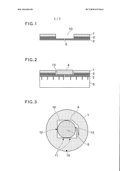
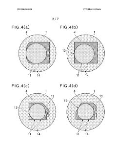
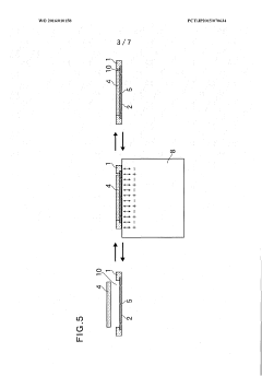
Semiconductor process carrier
PatentWO2016010158A1
Innovation
- A semiconductor process carrier using a transfer base member with a polyimide film and surface activation bonding by plasma irradiation, allowing for the secure attachment and detachment of small substrates via an electric field, enabling handling of small substrates without modifying the equipment, and accommodating various shapes and sizes, including high-temperature processing.
Method and station for treatment of a transport container made of plastic material for the atmospheric storage and conveyance of substrates
PatentInactiveEP3171992A1
Innovation
- A process involving a plasma treatment step under low gas pressure (<10,000 Pascal) is applied to the inner walls of the transport boxes, using a plasma of noble or reactive gases, with optional heating and intermittent plasma to enhance surface and volume decontamination, combined with infrared radiation and controlled gas pressure to accelerate contaminant elimination without degrading the plastic.
Environmental Impact of Plasma Processing Technologies
Plasma processing technologies, while essential for semiconductor manufacturing, present significant environmental challenges that require careful consideration. The cold plasma treatments used to modify semiconductor carrier transport properties involve various gases and energy inputs that can lead to environmental impacts throughout their lifecycle.
The primary environmental concern with plasma processing is the use of greenhouse gases such as perfluorocarbons (PFCs), sulfur hexafluoride (SF6), and nitrogen trifluoride (NF3). These gases have global warming potentials thousands of times greater than CO2 and can persist in the atmosphere for thousands of years. When used in cold plasma treatments for semiconductor modification, even small emissions can have disproportionate climate impacts.
Energy consumption represents another substantial environmental burden. Plasma generation requires significant electrical power, contributing to indirect carbon emissions depending on the energy source. Advanced cold plasma systems for precise carrier transport modification often demand even higher energy inputs to achieve the necessary precision and uniformity, further increasing the carbon footprint of semiconductor manufacturing processes.
Waste management challenges arise from byproducts of plasma reactions. The interaction between plasma and semiconductor surfaces generates potentially hazardous waste streams containing reactive species, particulates, and chemical compounds. These require specialized treatment and disposal protocols to prevent environmental contamination and human health risks.
Water usage and contamination present additional concerns. Cooling systems for plasma equipment and post-processing cleaning operations consume substantial water resources. The wastewater may contain trace amounts of chemicals and particles that require advanced treatment before discharge to prevent aquatic ecosystem damage.
The semiconductor industry has responded with several mitigation strategies. Point-of-use abatement systems can destroy or capture harmful emissions before they reach the atmosphere. Process optimization techniques reduce the required plasma treatment duration and intensity while maintaining the desired effects on carrier transport. Alternative chemistries with lower environmental impact are being developed to replace the most problematic gases.
Regulatory frameworks worldwide are increasingly addressing these environmental impacts. The Semiconductor Climate Consortium and the World Semiconductor Council have established voluntary reduction targets for greenhouse gas emissions, while governmental regulations in major manufacturing regions impose mandatory controls on emissions, waste handling, and resource consumption.
Integration Challenges with Existing Fabrication Processes
Integrating cold plasma treatment into existing semiconductor fabrication processes presents significant challenges that require careful consideration. The semiconductor industry has established highly optimized and standardized manufacturing processes, making any new technology integration complex and potentially disruptive. Cold plasma treatment, despite its promising effects on carrier transport properties, introduces several compatibility issues with conventional fabrication flows.
Temperature management represents a primary concern when incorporating cold plasma treatments. While "cold" plasma operates at lower temperatures than thermal plasma, the localized energy transfer can still create thermal gradients that may affect previously deposited materials or structures. Existing fabrication equipment is calibrated for specific thermal profiles, and introducing plasma treatments may necessitate recalibration or redesign of thermal management systems.
Equipment compatibility poses another substantial challenge. Most semiconductor fabs utilize standardized tools from established vendors, with production lines designed for specific process sequences. Introducing cold plasma treatment requires either retrofitting existing equipment or adding new specialized tools, both options demanding significant capital investment and potential production downtime.
Process sequence optimization becomes critical when integrating plasma treatments. The timing of plasma exposure within the fabrication flow significantly impacts its effectiveness on carrier transport. Determining the optimal process window—whether pre-metallization, post-oxide deposition, or at another stage—requires extensive experimentation and may vary depending on device architecture and target specifications.
Contamination control represents a persistent concern in semiconductor manufacturing, and plasma treatments introduce additional variables. Plasma species can potentially introduce unintended impurities or create surface states that interfere with subsequent process steps. Developing appropriate cleaning and passivation protocols becomes essential to maintain yield and reliability metrics.
Scalability challenges emerge when transitioning from laboratory demonstrations to high-volume manufacturing. Cold plasma treatments must demonstrate consistent results across large wafer areas and maintain reproducibility from wafer to wafer. The uniformity of plasma effects becomes increasingly difficult to maintain as wafer sizes increase to 300mm and beyond, potentially requiring innovations in plasma source design and distribution systems.
Metrology and quality control procedures need adaptation to effectively monitor plasma treatment outcomes. Conventional inspection techniques may not adequately capture the subtle changes in carrier transport properties, necessitating the development of specialized measurement protocols and acceptance criteria that can be integrated into existing quality management systems.
Unlock deeper insights with Patsnap Eureka Quick Research — get a full tech report to explore trends and direct your research. Try now!
Generate Your Research Report Instantly with AI Agent
Supercharge your innovation with Patsnap Eureka AI Agent Platform!